"The only way to meet the expectations placed on modern microelectronics is through networking and cooperation"
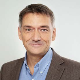
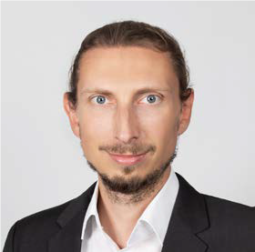
Microelectronics are a fundamental driver of innovative potential in numerous sectors. The Research Fab Microelectronics Germany (FMD) was created in 2017 to strengthen the position of Europe’s semiconductor and electronics industry on the global playing field. We spoke to the chair of FMD and spokesman of the Fraunhofer Group for Microelectronics, Professor Albert Heuberger, about FMD’s accomplishments so far and the expectations associated with modern microelectronics.
Professor Heuberger, the process of set�ting up FMD is largely completed. What has been achieved, and what’s next?
We’ve managed to complete the consider�able investments in infrastructure in the member institutes, with the exception of a few delays caused by the COVID-19 pan�demic. We are now in the process of imple�menting and establishing the Research Fab Microelectronics model. A first step has been taken with the reorganization of the admin�istrative office. Already, FMD is regarded as a paradigm for the deployment of diverse ex�pertise from different institutions united by a common strategy, offering complementary products and services to industry. Furthermore, we must continue to system�atically combine and strategically develop the expertise of our member institutes so as to maintain the technological sovereignty and the appeal of Germany and Europe for top-level research. It is important that we work purposefully and together on key fu�ture issues so as to be more agile than our competitors in the USA and Asia.
Many sectors are facing seismic changes as a result of digitalization. What chal�lenges will the field of microelectronics have to overcome?
Artificial intelligence (AI), Industry 4.0, driver�less cars – all of these digital developments require new methods, processes, and busi�ness models for the transmission, storage, and processing of large amounts of data. Existing computer technology can barely keep up with evolving demands in terms of energy consumption, data processing, and transfer speeds. As we become more de�pendent on digital networks and data, our security needs also become more sophisti�cated. A particularly crucial aspect in this regard is technological sovereignty, i.e., selfdetermination and control over systems and data in Germany and Europe. Until now, the market clout of primarily US-based IT corporations such as Microsoft and Google has led to virtually unavoidable dependen�cies. The same is true of chip manufactur�ing, which is primarily based in Asia. Trusted electronics and data security are at the heart of all digital networked systems – especially the Internet of Things, but also AI. Particularly in fields involving the pro�cessing of personal or security-critical data, such as medical technology, driverless cars or critical infrastructure, it is vital for own�ers to have full control over their ICT sys�tems and for users to receive information about the characteristics of the systems they are using. And this concerns the entire data flow – from the end customer to the actual hardware processing the data.
Can you give us any examples of how the FMD helps industry in this regard?
We design comprehensive, innovative elec�tronic systems for new research fields re�quiring this kind of wide-ranging expertise. I would like to name three examples. In the TRAICT (TrustedResourceAware ICT) project, eight FMD institutes collaborate with ten other Fraunhofer institutes to cre�ate the necessary framework conditions for trusted and data protection compliant in�formation and communication technology that can be used in a self-determined and secure manner. The key issue here is how to validate and safeguard the reliability of critical electronic components and systems in globally interconnected supply and value chains. Nowadays, many of the critical components in digital technologies are manufactured outside of Europe, and in many parts of the digital supply chain sup�pliers in other countries hold quasi-monop�olies. The result is a high level of dependen�cy that could become detrimental to Germany. In March, we launched the “Velek�tronik” platform for trusted electronics, the goal of which is to examine the entire value chain and devise coherent concepts. In all, 12 partners are involved in the proj�ect: 11 Fraunhofer and Leibniz institutes belonging to the FMD, and the edacentrum. They will develop and apply appropriate standards, norms, and processes on the basis of a national and European chip secu�rity architecture. Despite intensive efforts to design increas�ingly energy-efficient electronic compo�nents, primarily with the aim of increasing mobility supported by electronic devices, overall energy consumption by information and communication technology has contin�ued to rise. This problem is exacerbated by recent developments in the field of self�learning systems and their expected propa�gation into all areas of life and work. The upshot is that large data centers will no longer be solely responsible for the bulk of energy consumption, as increasingly preva�lent IoT devices and systems account for an ever greater share. More and more of the energy consumed will be due to the massive increase in data transmission. To address these challenges, the FMD is planning a competence center for resource-efficient in�formation and communication technology, or “Kompentenzzentrum Green ICT”.
We’re curious: You have been chair of FMD and spokesperson of the Group for Microelectronics for a little over a year. What has changed from your per�spective?
The past year has been filled with difficult challenges for all of us. The frequency of online meetings and the lack of personal contact with FMD colleagues has signifi�cantly affected my own working practices and culture. I am thankful that technology enables us to keep on working and stay in touch. My role as spokesperson involves some interesting duties, for instance in the executive board of the Fraunhofer-Gesell�schaft or in European bodies. I find it moti�vating that the significance of microelec�tronics for future issues like quantum technology or technological sovereignty is being acknowledged, and that I can person�ally play a part in shaping the changes un�derway in Germany’s research community.
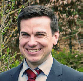
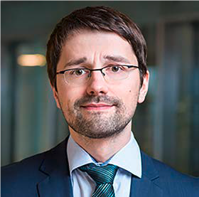
| Professor Heuberger has been execu�tive director of the Fraunhofer Insti�tute for Integrated Circuits IIS since 2011. Among other memberships, Professor Heuberger is a member of the Scientific and Technical Coun�cil of the Fraunhofer-Gesellschaft, a member of the board of the Medi�cal Valley Europäische Metropolregi�on Nürnberg (EMN) e.V., of the uni�versity council of Nuremberg Tech Georg Simon Ohm and of Coburg University of Applied Sciences and Arts as well as of the Communica�tion and Navigation program com�mittee of the German Space Agency DLR. In 2017, he was appointed as a member of acatech, the German National Academy of Science and Engineering. In 2019, he was awar�ded the Fraunhofer Medal for his ser�vices to the Fraunhofer-Gesellschaft. Professor Heuberger has been chair of FMD and spokesperson for the Fraunhofer Group for Microelectro�nics since 2020. |
The interview was conducted by Akvile Zaludaite.