Sensor Systems

FMD offers profound in-depth knowledge in manufacturing sensors and integration of sensors in complex systems:

  • Design of sensor systems, design for reliability and the test of sensor systems even under harsh environments
  • Fully integrated sensor solutions (MEMS on CMOS) as well as hybrid integrated sensor systems
  • Characterization (optical, acoustical, electrical) and test of sensors and sensor systems – with non-destructive methods as well as reliability assessments under multiple stress scenarios

Flyer Sensor Systems

Download Flyer


Theranostic Implants

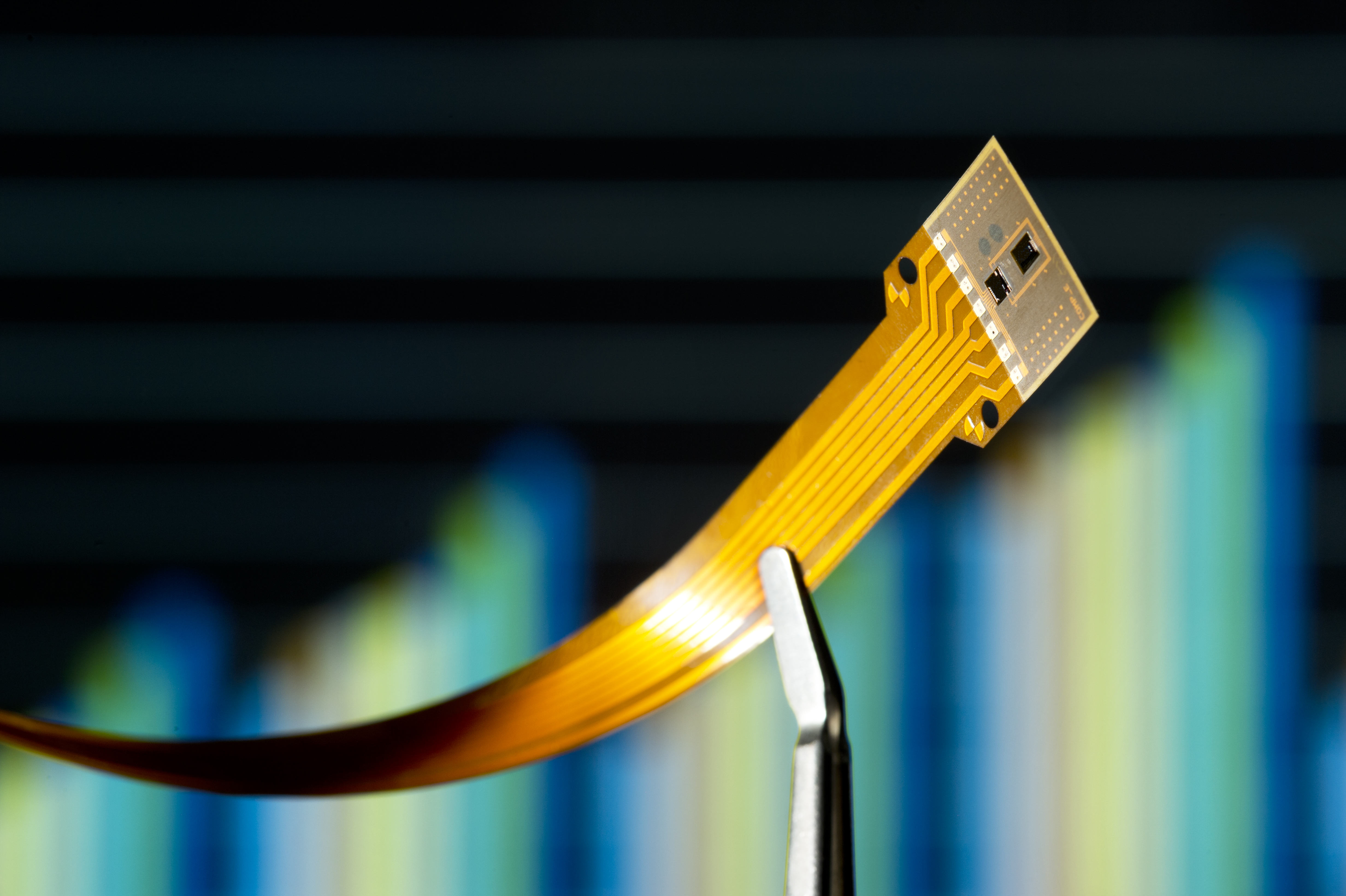
Overall system including pressure and acceleration sensor with a length of about 15 mm and a diameter of about 3 mm.


High-Voltage Power Grid Monitoring

Monitoring system for high and maximum voltage power grids.


Universal Sensor Platform (USeP)

Sensor Systems

With its 13 member institutes of the Fraunhofer-Gesellschaft and Leibniz Association, the Research Fab Microelectronics Germany (FMD) demonstrates research achievements of international excellence. In this way, FMD contributes to Germany and Europe taking a leading position in research and development. Some selected research highlights and lighthouse projects in the field can be found below.

SiC Pressure Sensor

© Fraunhofer IZM
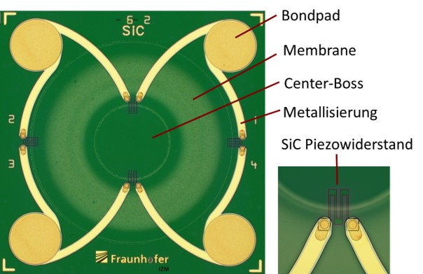
Top view of a SiC pressure sensor. The membrane was fabricated using RIE with a depth of 300µm and an etch rate of up to 4µm/min.
  • Fabrication of a pressure sensor made of EPI SiC specialized for the use in high temperature environments.
  • Reactive ion etching of SiC to produce the membrane of the pressure sensor up to a depth of 300µm
  • Etching speed of SiC is at 4µm/min

Publications:

  • Mackowiak P, et al. (2022): Investigation and Modeling of Etching Through Silicon Carbide Vias (TSiCV) for SiC Interposer and Deep SiC Etching for Harsh Environment MEMS by DoE, in IEEE Transactions on Components, Packaging and Manufacturing Technology, vol. 12, no. 3, pp. 437-445, March 2022. doi: 10.1109/TCPMT.2021.3123384
  • Mackowiak P, et al. (2021)Piezoresistive 4H-Silicon Carbide (SiC) pressure sensor, 2021 IEEE Sensors, pp. 1-4. doi: 10.1109/SENSORS47087.2021.9639506.
  • Erbacher K, et al. (2022): Investigation and Modeling of Etching Through Silicon Carbide Vias (TSiCV) for SiC Interposer and Deep SiC Etching for Harsh Environment MEMS by DoE, in IEEE Transactions on Components, Packaging and Manufacturing Technology, vol. 12, no. 3, pp. 437-445, March 2022. doi: 10.1109/MEMS51782.2021.9375268

3D Magnetic Field Cameras with Worldwide Unique Performance through Profilometer

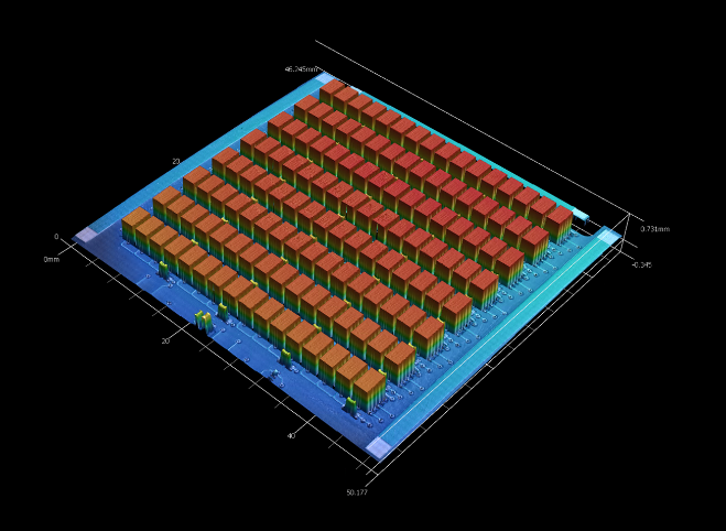
Schematic representation of a HallinSight® sensor array.
© Fraunhofer IIS
Schematic representation of a HallinSight® sensor array.
  • Development of magnetic measuring systems for the three-dimensional measurement of magnetic vector fields using in-house developed HallinOne® sensors
  • Production of magnetic field cameras (HallinSight®: vector magnetic field measurement) of a quality never seen before. Especially the alignment of the z-sensors serving as reference can be checked with this mechanical measurement and thus further optimized in several steps. In the end, this leads to vectorial measuring cameras whose alignment of the individual magnetic field sensors is very precise.
  • FMD-Investment "Laboratory for Nanooptical Structures" enables the alignment and positioning of many single chips on a PCB carrier; meaning, the precise measurement as well as correction and verification of the magnetic field values of the measuring system.

Cooperation: 

Projects with automotive suppliers

Further information: 

HallinSight®: Vectorial magnetic field measurement

Nano hollow needles for intracellular contacting

© Fraunhofer IMS
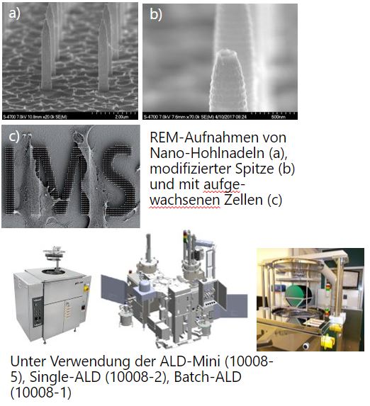
Translation: <> SEM images of nano hollow needles (a), modified tip (b) and with grown cells (c). <> Using the ALD-Mini (10008-5), Single ALD (10008-2), Batch ALD (10008-1)
  • Unique nano hollow needles fabricated on CMOS in sacrificial layer process and biocompatible ALD materials.
  • Novel capability for cell analysis: substance injection into the interior of the cell with simultaneous electrical analysis of the cell membrane potential

Publications:

Further Information: 

www.ims.fraunhofer.de/de/Geschaeftsfelder/Devices-and-Technologies/Anwendungen/ZellMOS.html

High-Resolution Imaging using SAR and ISAR Techniques

© Fraunhofer FHR
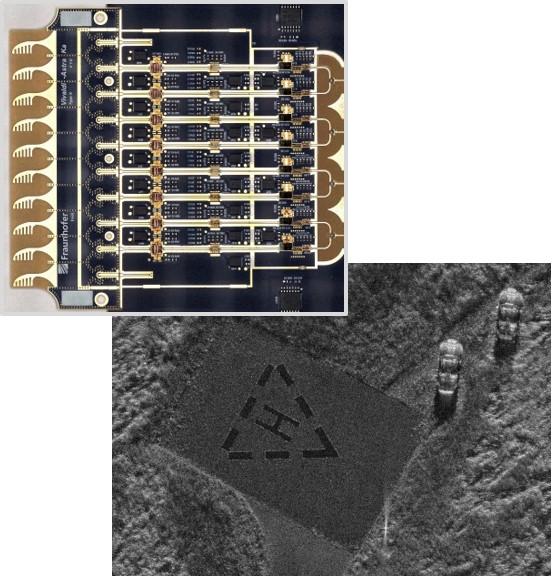
Figure 1: Compact Ka-band phased array radar sensor with a system bandwidth of 8 GHz for airborne systems. Figure 2: SAR image of a ground scene (helipad and vehicles) with a processed resolution of 2 x 2 cm.
  • Complex multifunctional radar sensor technology for high-resolution SAR imaging of ground scenarios and of objects in low-Earth orbit
  • Frequency bands used from X-band to terahertz
  • World's first SAR images at 300 GHz with millimeter resolution
  • Applications on moving and flying platforms with motion compensation
  • Sensor technology applicable for further complex radar tasks such as GMTI, change detection and 3D scene detection by interferometry (IFSAR)
  • High-resolution and long-range 2D and 3D imaging of moving objects using the special procedures ISAR and interferometric ISAR

Publication:

  • Palm S, et al. (2018): Mobile Radar Mapping—Subcentimeter SAR Imaging of Roads, in IEEE Transactions on Geoscience and Remote Sensing, vol. 56, no. 11, pp. 6734-6746, Nov. 2018. doi 10.1109/TGRS.2018.2842643
  • Palm S, et al. (2019): Airborne Circular W-Band SAR for Multiple Aspect Urban Site Monitoring, in IEEE Transactions on Geoscience and Remote Sensing, vol. 57, no. 9, pp. 6996-7016, Sept. 2019. doi: 10.1109/TGRS.2019.2909949
  • Walterscheid I, et al. (2020): First results of a joint measurement campaign with PAMIR-Ka and MIRANDA-94, in IEEE Radar Conference (RadarConf20), Sept. 2020. doi: 10.1109/RadarConf2043947.2020.9266536
  • El-Arnauti G, et al. (2018): Advanced System Concept and Experimental Results of the Ultra-High Resolution Airborne SAR Demonstrator PAMIR-Ka, VDE, in EUSAR 2018 - 12th European Conference on Synthetic Aperture Radar. Print ISBN:978-3-8007-4636-1

Further information: 

300-GHz SAR measurements of streets and facades

Photodetectors for Highly Dynamic Three-Dimensional Imaging - Even in Changing Weather Conditions

CSPAD detector: These photodetectors combine highly dynamic three-dimensional imaging with reliable algorithms for high-performance use even in changing weather conditions.
© Fraunhofer IMS
CSPAD detector: These photodetectors combine highly dynamic three-dimensional imaging with reliable algorithms for high-performance use even in changing weather conditions.

Modern driver assistance systems require efficient and reliable sensor technology. Autonomous vehicles must be able to detect their surroundings with absolute certainty. For this purpose, CSPAD detectors combine highly sensitive three-dimensional imaging with reliable algorithms for high-performance operation even under changing weather conditions, e.g. for use in LiDAR applications.

  • Maximum ranges even with high sunlight intensity and low system costs at the same time
  • Integration of the SPAD detectors in a 0.35 µm CMOS process certified for the automotive industry and optimized for optoelectronic applications
  • In-pixel integrated adaptive photon coincidence circuit for background light suppression

Cooperations:

Publications: 

  • Ruskowski J, et al. (2020): 64x48 pixel backside illuminated SPAD detector array for LiDAR applications, in SPIE Photonics West 2020, SPIE Opto; USA. doi: 10.1117/12.2550634
  • Kalwa L, et al. (2019): Wafer-Level-3D-Integrationsverfahren für hochsensitive optische Sensoren, in 20. GMA/ITG Fachtagung Sensoren und Messsysteme 2019; Germany. doi: 10.5162/sensoren2019/3.2.3

Further information: 

Technologies in the Business Unit CMOS Image Sensors