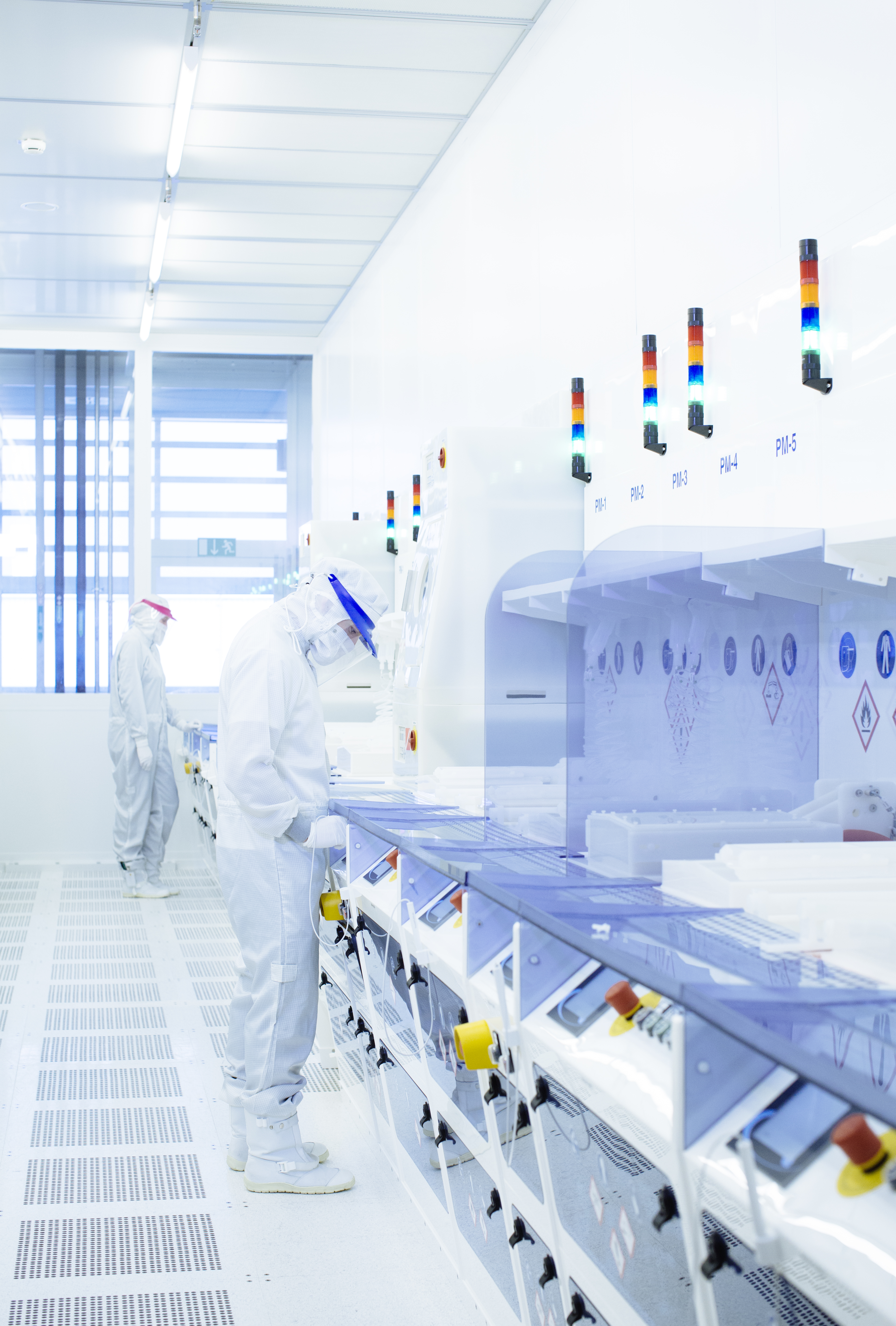
Cleanroom Facilities

FMD Cleanrooms in a nutshell
Privacy warning

With the click on the play button an external video from www.youtube.com is loaded and started. Your data is possible transferred and stored to third party. Do not start the video if you disagree. Find more about the youtube privacy statement under the following link: https://policies.google.com/privacy

2.200 machines in 13 cleanrooms throughout Germany

More than 19.500 m2 cleanroom space

More than 10 million moves per year

Wafer-sizes from 2“ to 300 mm

Semiconductor materials from Si over SiGe to Compound Semiconductors like SiC, GaN, GaAs, InP and many more

Overview: Processing Capabilities within FMD

Download

Overview of the FMD Cleanrooms

Technological Highlights

7 Cleanrooms, partly with Automotive Certification,

200 mm BiCMOS/CMOS Lines, incl. FEOL and BEOL Module,

Special technologies like HV CMOS and high temperature CMOS (up to 300°C),

Interface to Foundry Companies,

300 mm Material, Process and Equipment screening Line,

200 mm / 300 mm Packaging Lines,

Automated Inline Process Monitoring,

Frontend and Backend Contamination Management and Control,

Single process developments and optimizations like Etching, ALD/ALE, Wet Cleaning, Annealing, Epitaxy (Si, SiGe), Implantation, CMP and many more.

Our know-how in detail

200 mm

Fraunhofer IISB, 200 mm Si Line

more than 1500 m2 cleanroom space - ISO 4 

Fraunhofer EMFT, ≤ 200 mm CMOS Line

ca. 1000 m2 cleanroom space - ISO 4


Fraunhofer IMS, 200 mm CMOS Line

more than 1500 m2 cleanroom space - ISO 4

Fraunhofer ISIT 200 mm Si Line

more than 1500 m2 cleanroom space - ISO 4 / 5


Leibniz IHP, 200 mm (Bi)CMOS Line

ca. 1000  m2 cleanroom space - ISO 1

Europractice IC Service


Fraunhofer IZM-Berlin 100 - 300 mm Packaging Line

more than 1500 m2 at both locations - ISO 6


300 mm

Fraunhofer IPMS 300 mm Screening FAB
2700 m² of class 6 and 3 cleanroom space (in accordance with ISO 14644-1) and laboratory space for over 80 processing and analytical tools

Fraunhofer IZM-ASSID 200 - 300 mm Packaging Line
ca. 800 m2 cleanroom space - ISO 6


Technological Highlights

6 Cleanrooms with 200 mm MEMS-Lines and Foundry

Interface to Foundry Companies

Selected Processes on 300 mm Wafer diameter

200 / 300 mm Packaging Lines

Frontend and Backend Contamination Management and Control

Single Process Developments and Optimizations like Etching, ALD/ALE, Wet Cleaning, Piezo Materials and many more

Unser Know-how im Detail

200 mm

Fraunhofer ENAS ≤200 mm MEMS and sensor Line
ca. 1000 - 1500 m2 cleanroom space - ISO 4 / 6

Fraunhofer IMS 200 mm MEMS Line
ca. 1300 m2 cleanroom space - ISO 4

Fraunhofer IPMS 200 mm MEMS Line
more than 1500 m2 cleanroom space combined at 2 locations - ISO 4

Fraunhofer ISIT 200 mm MEMS Line
more than 1500 m2 cleanroom space - ISO 4 / 5

Fraunhofer IZM-Berlin 200 mm Packaging Line
more than 1500 m2 at both locations - ISO 6


Fraunhofer IZM-Berlin 200 mm Packaging Line

more than 1500 m2 at both locations - ISO 6


300 mm

Fraunhofer IZM-ASSID 300 mm Packaging Line

ca. 800 m2 cleanroom space - ISO 6


Technological Highlights

SiC-Prototype-Foundry: Production of Silicon Carbide-devices with wafer sizes from 100 mm to 150 mm at Fraunhofer IISB

InP Foundry: InP-Processing up to 4” at Fraunhofer HHI, and Leibniz FBH and InP-based Photonic-Integrated Circuits at Fraunhofer HHI

GaN-on Si 200 mm at Fraunhofer IAF & ISIT

III-V-Semiconductors: GaAs,  InxGa1-xAs,  InxGa1-xAsyP1-y,  InP,  GaN,  AlGaN,  AlN, AlScN, GaSb and more

Our know-how in detail

Up to 4" Compound Semiconductors

Leibniz FBH up to 100 mm Compound Semiconductors
ca. 2700 m2 cleanroom space - ISO 5 / 6


Fraunhofer HHI up to 100 mm Compound Semiconductors

ISO 4 / 6

Fraunhfoer IAF up to 100 mm Compound Semiconductors and WBG materials

ca. 1000 m2 cleanroom space - ISO 3 / 4

Up to 6" Compound Semiconductors

Fraunhofer IISB 150 mm SiC Line
more than 1500 m2 cleanroom space - ISO 4


Up to 8" Compound Semiconductors

Fraunhofer IAF (ISO 3 / 4) and ISIT (ISO 4 / 5) 200 mm GaN-on-Si Line (in Cooperation)

combined more than 2500 m² cleanroom space