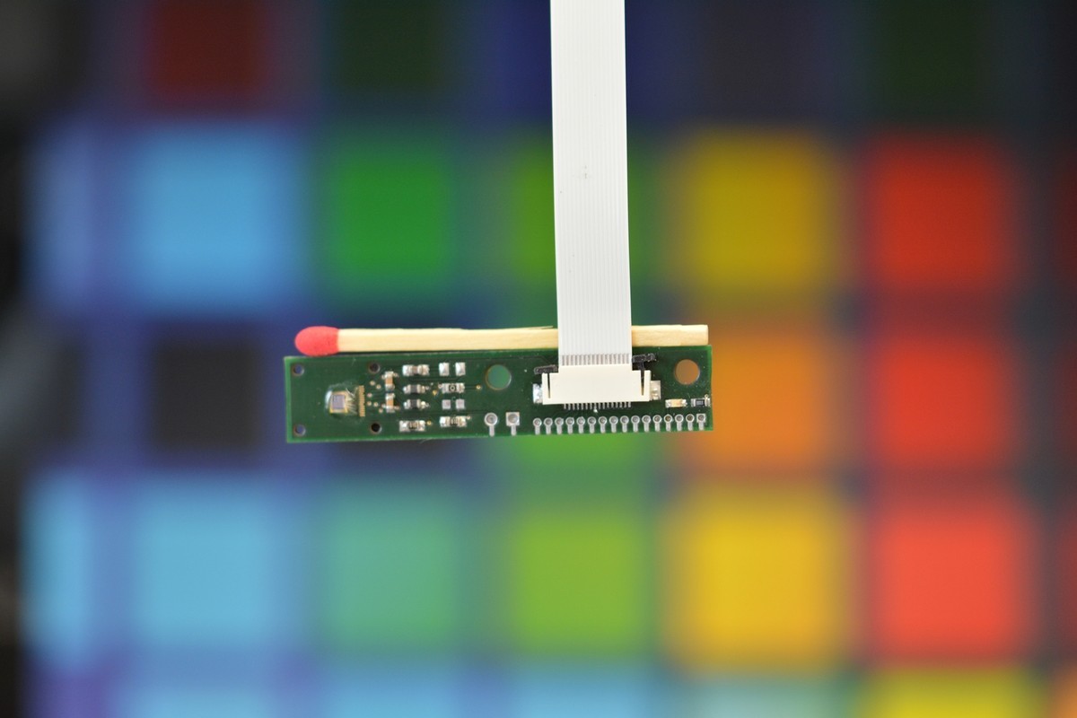
The technology platform "Optoelectronic Systems" focuses on the realization of optoelectronic devices and systems-on-chip. Applications include image acquisition and processing as well as communication up to Tbit/s-speed, Raman spectroscopy under strong scattered light conditions, and quantum optical sensors and measurement technologies for optical atomic clocks, for ground-based as well as space-based applications. From one single source, we offer the complete component and technology chain, e.g. for optical communication from emitter to modulator and receiver to fully integrated optoelectronic systems, including application-specific instruction-set processor based control and embedded software for these technologies.

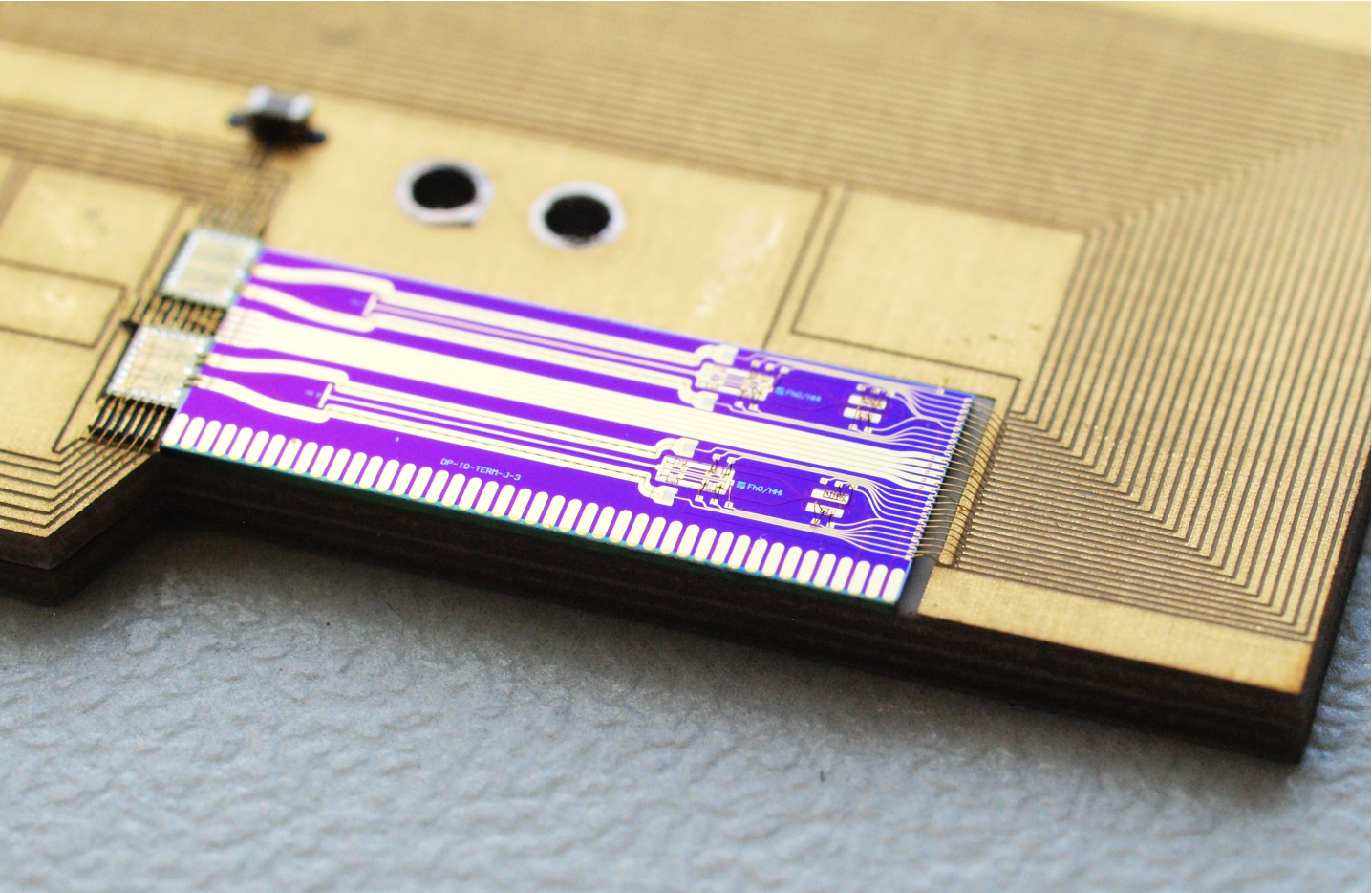
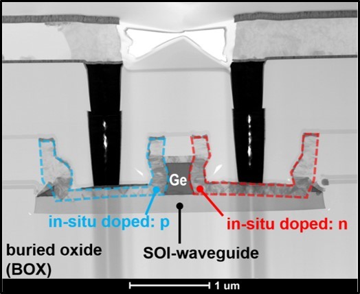
Furthermore, the hybrid integration of active III-V-materials to polymer- and Si-based technology, incl. wafer level atomic layer deposition for encapsulation, plays a significant role in order to realize complete hybrid photonic integrated circuits (Hybrid PICs).


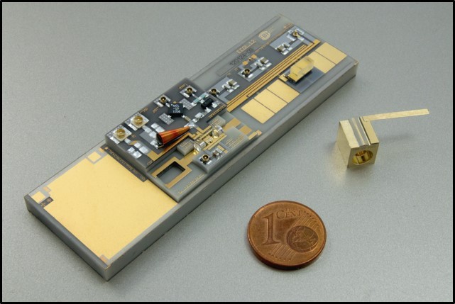
Realization of Optoelectronic Systems such as for communication up to Tbit/s-speed

Complete Signal Chain from emitter to modulator and receiver to fully integrated optoelectronic systems

Design of Single Devices, (integrated) Circuits or even Complete Systems, such as communication systems

In-depth knowledge in Processing a wide variety of Materials – from Si to compound semiconductors and polymers

Manufacturing of Passive Structures, like anti-reflection coatings and Laser; wide ranging Portfolio of different Laser Wavelengths: GaAs-based Laser (wavelength 620 – 1180 nm), InP-based Laser (~ 1.5 µm) and III-V-semiconductor Laser with wavelengths in the range of 2-11 µm

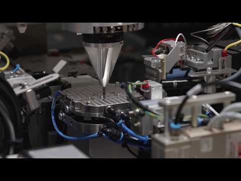
Integration of III-V-Materials into Si-based Technology; heterogeneous integration: Advanced Packaging, Wafer Level Capping & Advanced Substrate/Interposer technologies

Characterization of the designed, manufactured and assembled optoelectronic systems and testing in multiple stress scenarios (thermal or mechanical stress); performing reliability and degradation assessments.

Flyer Optoelectronic Systems

Download Flyer


External Cavitiy Quantum Cascade Lasers

for completely new ways of infrared spectroscopy.


Tunable Laser Module

for a broad range of application fields.


Implementation / Coupling of a Photonic Integrated Circuit

from the cooperation in the BMBF project SPeeD


Laser Modules for Space Applications

Successfully used in space: a micro-integrated diode laser module

Packaging and Interconnection Technology for Optoelectronic Systems

With its 13 member institutes of the Fraunhofer-Gesellschaft and Leibniz Association, the Research Fab Microelectronics Germany (FMD) demonstrates research achievements of international excellence. In this way, FMD contributes to Germany and Europe, taking a leading position in research and development. Some selected research highlights and lighthouse projects in the field of packaging and interconnection technology for optoelectronic systems can be found below.

Heterogeneous integration for optical applications

© Fraunhofer ISIT
In-situ laser soldering allows heterogeneous integration of optical components, e.g. for extremely miniaturized laser light sources and laser scanners. Glass caps can be manufactured in various shapes.
Heterogeneous 3D microintegration for optical applications
  • Silicon wafer as optical bench for heterogeneous 3D microintegration of laser light sources and MEMS mirrors with active lens alignment
  • Modular glass-silicon packaging platform enables hermetic packaging of active and passive optical devices in defined atmosphere without organic outgassing
  • Process development for in-situ laser soldering through different substrates e.g. silicon and glass
  • Development of the world's smallest RGB laser light source

Cooperations:

BMBF funded project "PRISMA"

DLR Project proposal "MEMS-BORO"

Publications:

  • Reinert W, Malaurie P (2020): A miniaturized RGB-laser light engine, in: Components and Packaging for Laser Systems VI, 1126117 (21 February 2020). doi: 10.1109/ESTC48849.2020.9229809
  • Stenchly V, et al. (2017): Modular packaging concept for MEMS and MOEMS, in: J. Phys.: Conf. Ser. 922 012015 (2017). doi: 10.1088/1742-6596/922/1/012015

Further information:

www.isit.fraunhofer.de/en/micro-fabrication-technologies.html

Narrowband diode laser (ECDL)

© Leibniz FBH
  • World's first integration of a narrowband ECDL (extended cavity diode laser) on a single GaAs opto-electronic device using a unique GaAs growth and fabrication technology
  • Demonstration of the monolithic diode laser with the narrowest bandwidth in the world
  • Close integration of actors along the value chain, from simulation and design to semiconductor technology and extensive opto-electronic measurement technology

Cooperations:

  • DLR (BMWi), group project ROSC, sub-project mECDL
  • DLR (BMWi), group project SOLIS

Publications:

  • Brox O, et al. (2021): Novel 1064 nm DBR lasers combining active layer removal and surface gratings, in: Electron. Lett. 57, 559-561, Mai (2021). doi: 10.1049/ell2.12192
  • Wenzel S, et al. (2021): Ultra-narrow linewidth GaAs-based DBR Lasers, in: Conf. on Lasers and Electro-Optics (CLEO 2021), virtual event, p. ATh4G.3 (Mai 2021). Online abrufbar unter: https://opg.optica.org/abstract.cfm?uri=CLEO_AT-2021-ATh4G.3

Further information:

 Joint Lab Quantum Photonic ComponentsOptoelectronics Department

Fabry-Pérot-Interferometer and Hyperspectral Imaging​

© Fraunhofer IIS / EAS
Examples of electrically tunable MOEMS bandpass filters for the visible (top-left) and infrared spectral range (right) successfully implemented at Fraunhofer ENAS. Their use addresses both infrared spectral sensing (e.g.: gas analysis) and hyperspectral imaging (bottom-left, source: Fraunhofer IIS/EAS). The FMD investments and associated acquisitions make a significant contribution in the implementation and optical characterization of optical filters and their further development.
  • Optical apertures up to 9 x 9 mm²
  • Electrically tunable MOEMS bandpass filters for the visible and infrared spectral range

Kooperationen:

  • M³Infekt (Fraunhofer project, FMD institute Fraunhofer ENAS in cooperation with FMD Institute Fraunhofer IIS/EAS)​
  • SAB: Minimodul

Veröffentlichungen:

  • Helke C, et al. (2019): VIS Fabry-Pérot Interferometer with structured (TiO2/PE-SiO2)³ Bragg-reflectors on 5 mm large LP-Si3N4 membranes, in Proceedings Volume 10931, MOEMS and Miniaturized Systems XVIII; 109310Q, SPIE OPTO, 2019, San Francisco, California, United States. doi: 10.1117/12.2509170
  • Hiller K. et al. (2019): Mikro- und Nanotechnologien zur Herstellung steuerbarer optischer Filter, in MikroSystemTechnik 2019 - Kongress. ISBN: 978-3-8007-5090-0
  • Ebermann M, et al. (2019): Next Generation of highly miniaturized Bulk-MEMS-Fabry-Pérot Filters for infrared Microspectrometers, in 2019 20th International Conference on Solid-State Sensors, Actuators and Microsystems & Eurosensors XXXIII (TRANSDUCERS & EUROSENSORS XXXIII). doi: 10.1109/TRANSDUCERS.2019.8808566

Further information:

Fabry-Pérot interferometer for sensor applications in the infrared spectral range on their way to further miniaturization

Chipsize spectrometer for analytics

© Fraunhofer IIS
Highly integrated and cost-effective chip-size spectrometer.
  • World's first commercialization of CMOS multispectral sensors based on plasmonic nanostructures
  • Uses optical nanostructures as spectral filters
  • Highly integrated and cost-effective spectral sensors for analytics

Cooperations:

BMBF supported project INFIMEDAR
 

Publications:

Further information:

www.iis.fraunhofer.de/en/ff/sse/sensor-solutions/optischesensorik.html

Very High-Speed Germanium Photo Detectors

© Leibniz IHP
  • Novel concept for the realization of waveguide-coupled germanium photodiodes, in which two complementary in-situ doped silicon layers enclose undoped germanium
  • Opto-electrical -3 dB bandwidths >110 GHz with high responsivity rates of 0.6 A/W were succesfully achieved (1550 nm wavelength)
  • Most advanced waveguide-coupled germanium photodiode to date

Cooperations:

  • EU funded project plaCMOS, Grant ID: 780997
  • BMBF funded project PEARLS, 13N14936

Publications:

  • Lischke S, et al. (2020): Ge Photodiode with -3 dB OE Bandwidth of 110 GHz for PIC and ePIC Platforms, in 2020 IEEE International Electron Devices Meeting (IEDM), 2020, pp. 7.3.1-7.3.4. doi: 10.1109/IEDM13553.2020.9372033
  • Lischke S et al. (2021) (invited): Very High-Speed Waveguide Integrated Germanium Photo Detectors, in 2021 European Conference on Optical Communication (ECOC). doi: 10.1109/ECOC52684.2021.9606091
  • S. Lischke et al. (2021): Waveguide-Coupled Ge Photodiodes with 3-dB Bandwidth >110 GHz, in 2021 IEEE Photonics Conference (IPC). doi: 10.1109/IPC48725.2021.9593030

80 GHz Flip-Chip integration of large InP-PICs on flexible substrates

© Fraunhofer HHI
Planarized RF contacts on InP MZM-PIC (left) for flip-chip integration of optical DAC (right)
  • World's first flip-chip integration of large InP-PICs on foldable polyimide (PI) substrates
  • Bandwidths > 80 GHz feasible
  • Integration of complex optoelectronic systems
  • Novel and energy-saving components feasible

Cooperations:

Publications:

  • Aimone A, et al. (2018): Programmable Transfer Function Optical-DAC Using an InP Segmented Mach-Zehnder Modulator,  in 2018 20th International Conference on Transparent Optical Networks (ICTON). doi: 10.1109/ICTON.2018.8473731
  • Palavesam N, et al, (2021): Advanced integration technology for fabricating high-speed electro-optical sub-assembly, in 2021 23rd European Microelectronics and Packaging Conference & Exhibition (EMPC). doi: 10.23919/EMPC53418.2021.9584968

Further information:

www.hhi.fraunhofer.de/en/departments/pc/research-groups/modulators.html

Industry-ready terahertz sensor technology up to 6 THz

© Fraunhofer HHI
© Fraunhofer HHI
Terahertz measurement platform from 0.2 - 6.0 THz.
  • Contact-free coating thickness measurement in multiple coating layers
  • Up to five layers with a minimum layer thickness of 5 µm with 0.2 µm accuracy
  • Analysis of ICs at terahertz frequencies

Cooperations:

Publications:

  • Liebermeister L, et al. (2021): Optoelectronic frequency-modulated continuous-wave terahertz spectroscopy with 4 THz bandwidth, in Nature Communications volume 12, Article number: 1071 (2021). doi: 10.1038/s41467-021-21260-x
  • Kohlhaas R B, et al. (2020): 637 μW emitted terahertz power from photoconductive antennas based on rhodium doped InGaAs, in Appl. Phys. Lett. 117, 131105 (2020). doi: doi.org/10.1063/5.0020766
  • Globisch B, et al. (2020): Fully Automated Terahertz Layer Thickness Measurement System, in 2020 45th International Conference on Infrared, Millimeter, and Terahertz Waves (IRMMW-THz). doi: doi.org/10.1109/IRMMW-THz46771.2020.9370502

Further information:

Terahertz Sensors and Systems @ Fraunhofer HHI

High-Precision Flip-Chip Bonding for Photonic Systems

© Fraunhofer IZM
FlipChip Bonder SET FC300: Accuracy of 1 µm at wafer level (factor 3 compared to the actual state) 
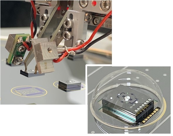
to achieve the hybrid integration of microelectronic, power electronic, photonic and sensor components on silicon wafers for further 3D integration.

The metallic micro-bumps are used to perform FlipChip assembly processes of the highest precision and the highest electrical connection density.

  • Demonstration of FlipChip Bonding in 3 µm pitch for optoelectronics (in cooperation with an international partner) with submicrometric postbond alignment
  • Demonstration of heterogeneous/hybrid silicon photonics Co-integration of InP-based and Si-based devices for highly packaged transceivers on silicon bench/submount in micrometric distance for photonic applications

Cooperations:
EU project 5G-PHOS (H2020)
 

Publication:
Papaioannou S, et al. (2018):  5G mm Wave Networks Leveraging Enhanced Fiber-Wireless Convergence for High-Density Environments: The 5G-PHOS Approach, in 2018 IEEE International Symposium on Broadband Multimedia Systems and Broadcasting (BMSB), Valencia, 2018, pp. 1-5. doi: 10.1109/BMSB.2018.8436713

Flip-Chip Interface for the Hybrid Integration of InP Components for Silicon Photonics

Privacy warning

With the click on the play button an external video from www.youtube.com is loaded and started. Your data is possible transferred and stored to third party. Do not start the video if you disagree. Find more about the youtube privacy statement under the following link: https://policies.google.com/privacy

Using the example of the Pic&Place machine installed at Fraunhofer HHI for hybrid integration of InP and Si or polymer components, we would like to show how local investments are used to expand the technological capabilities of the institutes and thus stimulate cross-disciplinary collaboration. For more information, watch the video.

  • The world's first flip-chip integration of InP components into SiN-TriPleX photonic integrated circuits
  • New, patented InP components with high-precision contact surfaces for passive vertical adjustment
  • Development of an innovative process for active adjustment by means of spatially resolved reflectometry

Cooprations:
BMBF-funded project PolyPhotonics Berlin
EU projekt UNIQORN (H2020)
EU projekt Teriphic (H2020)

Publications:

  • Theurer M, et al. (2020): Flip-Chip Integration of InP to SiN Photonic Integrated Circuits, in JOURNAL OF LIGHTWAVE TECHNOLOGY, VOL. 38, NO. 9, MAY 2020. doi: 10.1109/JLT.2020.2972065
  • Theurer M, et al. (2019): Actively aligned flip-chip integration of InP to SiN utilizing optical backscatter reflectometry, in Proc. ECOC, Dublin, Ireland, Sep. 2019, Paper W.2.B. 10.1049/cp.2019.0913
  • Conradi H, et al. (2020): Hybrid integration of a polarization independent circulator, in Proc. SPIE 11283, Integrated Optics: Devices, Materials, and Technologies XXIV, 112830J. doi: 10.1117/12.2545592
  • Kleinert M. et al. (2019): A platform approach towards hybrid photonic integration and assembly for communications, sensing, and quantum technologies based on a polymer waveguide technology, in 2019 IEEE CPMT Symposium Japan (ICSJ), Kyoo (Japan). doi: 10.1109/ICSJ47124.2019.8998655