Extended CMOS

The technology platform Extended CMOS focuses on materials and processes, system integration as well as characterization of materials, test of devices and reliability assessments.


The FMD offers long lasting experience and know-how in developing and manufacturing of CMOS-based components and systems within its cleanrooms:

  • Fully equipped state-of-the art 200 mm BiCMOS and CMOS lines
  • Processes for FEOL, MOL, as well as BEOL
  • New materials, processes and technologies, like new memory concepts and neuromorphic computing technologies are pursued
  • 1D, 2D materials and technologies; 2.5/3D integration technologies
  • R & D services for TSV, wafer bumping, redistribution layers and solder balls
  • Fabrication of high density silicon, glass and polymer interposer, wafer thinning, dicing, wafer to wafer bonding, high precision multi-die assembly, die stacking, and molding

Extended CMOS along the value chain


Europractice IC Service: Multi Project Wafer (MPW) and Prototyping 

Within the EUROPRACTICE IC Service, the Leibniz IHP as part of the Research Fab Microelectronics Germany, is providing a manufacturing service for Multi Project Wafer (MPW) and Prototyping. More information here.

Flyer Extended CMOS

Download Flyer


Universal Sensor Platform (USeP)

Extended CMOS

With its 13 member institutes of the Fraunhofer-Gesellschaft and Leibniz Association, the Research Fab Microelectronics Germany (FMD) demonstrates research achievements of international excellence. In this way, FMD contributes to Germany and Europe, taking a leading position in research and development. Some selected research highlights and lighthouse projects in the field of Extended CMOS can be found below.

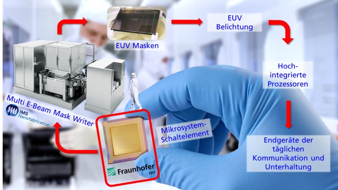
Monolithic integration for MEMS on CMOS: microsystem switching element for an electron multibeam mask writer

© Fraunhofer ISIT
Circuit of action: The microsystem switching element for an electron multibeam mask writer, manufactured at Fraunhofer ISIT, enables, among other essential core elements, the current progress in semiconductor manufacturing -> which includes the realization of 7nm, 5nm and 3nm technology nodes in the leading-edge area.
  • Microsystem switching element for an electron multi-beam mask writer which allows the realization of structures below 10 nanometers and less with EUV lithography production.
  • The heart of the mask writer is a MEMS microsystem switching element from Fraunhofer ISIT. 
  • The process is unrivaled so far - and it is indispensable if one wants to expose todays smallest achievable structures on microchips with EUV techniques.
  • Technology areas: MEMS post-processing on CMOS wafers, monolithic integration

Cooperation

Industry partner: IMS Nanofabrication GmbH, Vienna

Veröffentlichungen

Press information: Smaller, more powerful and unrivaled

Further information

TROM2-Chip: A chip for mask production

Joseph-von-Fraunhofer-Price: Film for the award win; microchips for the production of semiconductors: https://www.youtube.com/watch?v=KX8EE7hjI1E

Behind-the-scenes of the film: https://www.youtube.com/watch?v=HtWazFeLmtM

Fraunhofer Research Awards Ceremony 2021

www.isit.fraunhofer.de/en/news/fraunhofer-award-2021.html

First hybrid computer chip based on motor proteins

© Fraunhofer ENAS
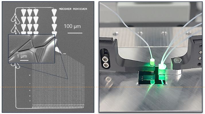
Left: Network of biofunctionalized nanochannels and logic crossings to compute an Exact Cover problem with 1024 possible solutions. Right: Functionalization and operation of the chips is realized by means of a microfluidic set-up
  • New processing capabilities for efficient nanostructuring of various biocompatible materials
  • World's first chip that uses motor proteins and biological agents to compute a mathematical problem of exact coverage with 1024 possible solutions

Cooperations:

  • EU supported project [bio4comp.org] (H2020)
  • TU Dresden, University Lund, Linneaus University, Bar Ilan University
  • Molecular Sense Ltd.

Publications:

  • Heldt G, et al. (2018): Approach to combine electron-beam lithography and two-photon polymerization for enhanced nano-channels in network-based biocomputation devices, doi: 10.1117/12.2326598
  • Meinecke C, et al. (2018): Nanofabricated Networks used for Protein-Powered Biocomputation Devices, in CAS 2018, 41st International Semiconductor Conference, Sinaia, Romania, 2018 Oct 10-12
  • Selbmann F, Meinecke C. et al. (2020): Parylene C Based Adhesive Bonding on 6" and 8" Wafer Level for the Realization of Highly Reliable and Fully Biocompatible Microsystems, in ECS Trans. 98 55. doi: 10.1149/09804.0055ecst


Non-Volatile Memories

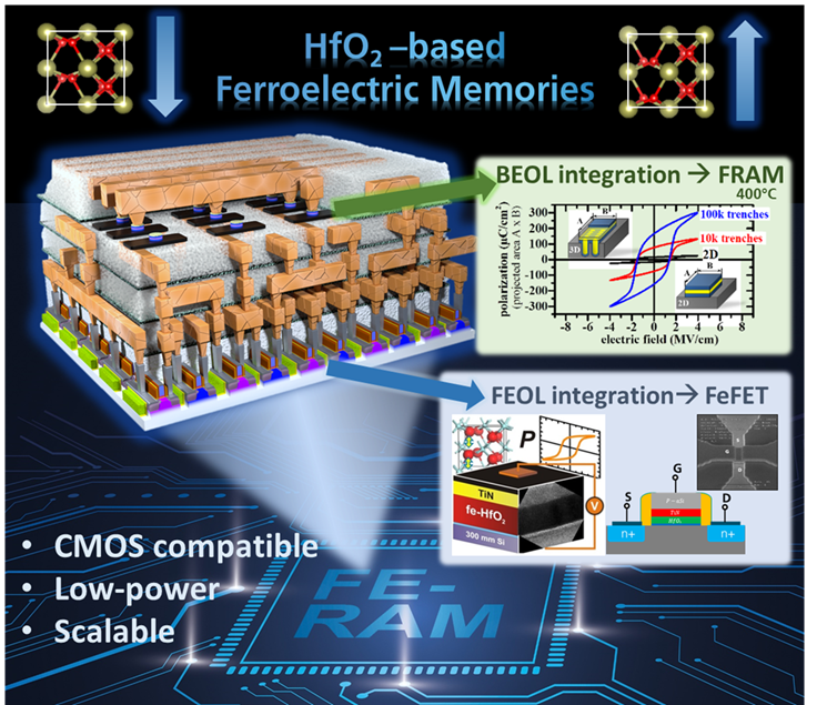
By means of ferroelectric field effect transistors (FeFET) based on HfO2 in the 28- or 22-nm technology node, the weight values required for deep learning algorithms can not only be stored directly in the chip but also calculated with these.
© Fraunhofer IPMS
By means of ferroelectric field effect transistors (FeFET) based on HfO2 in the 28- or 22-nm technology node, the weight values required for deep learning algorithms can not only be stored directly in the chip but also calculated with these.
  • Functional low-power memory solutions based on ferroelectric hafnium oxide (FeFETs, FRAM)
  • Integrated FeFET arrays in collaboration with GLOBALFOUNDRIES
  • Demonstration of the outstanding properties of circuits based on FeFETs for neuromorphic computing

Cooperation:

»RASCAL« (Racetrack Memory Scaling of ultra-dense and energy-efficient data storage)

  • Joint project of the Fraunhofer-Gesellschaft and Max Planck Society for material investigations and realization of racetrack memories using the FMD sputtering cluster
  • Goal is to demonstrate data storage technology with high reliability, scaling density, and energy efficiency

Weiterführende Informationen:
300 mm Devices and Value Added Solutions


Carbon Nanotubes (CNT) for Future Electronics and Sensor Technology

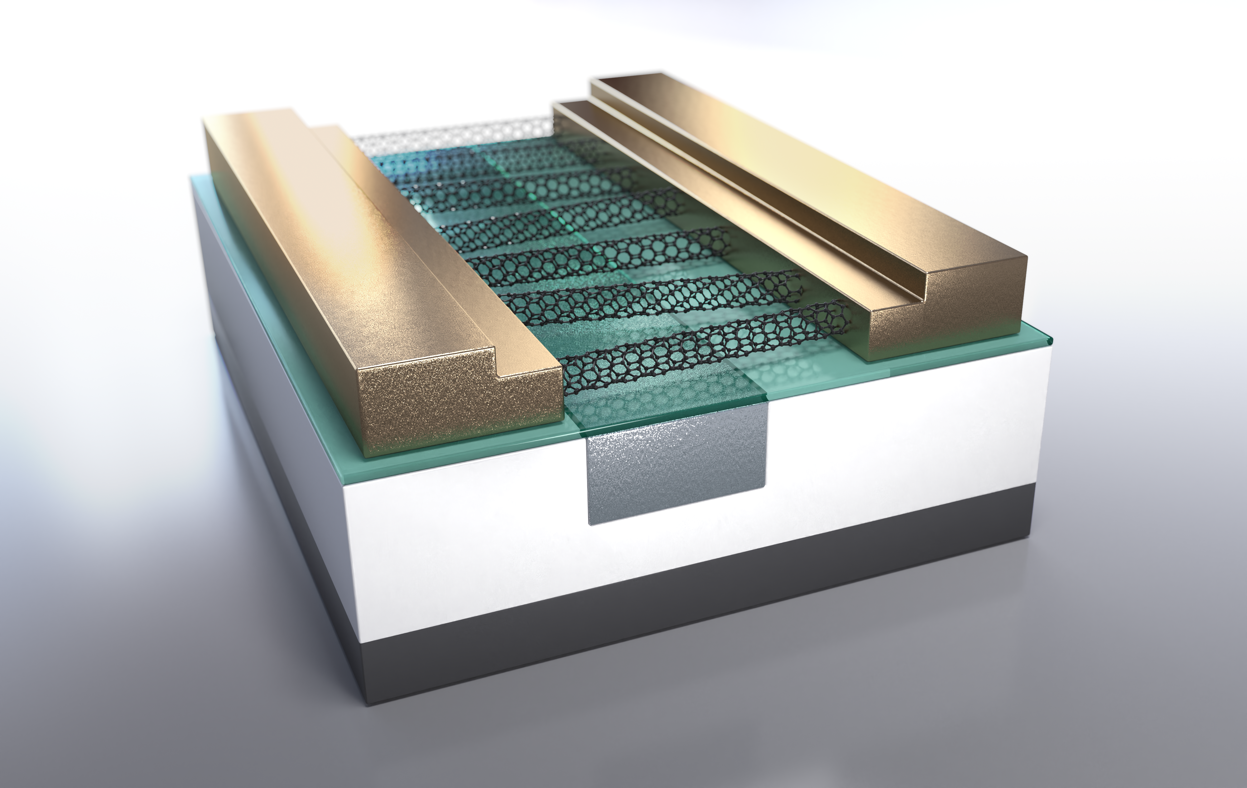
Schematic representation of a carbon nanotube based field effect transistor (CNT-FET).
© Fraunhofer ENAS
Schematic representation of a carbon nanotube based field effect transistor (CNT-FET).
  • On-Demand: First accessible platform for applications in (integrated) sensor technology
  • Heterogeneous integration technologies for nano-components consistently on wafers up to 200 mm (e.g. ASIC+CNT)
  • New technology for energy-efficient analog high-frequency transceiver electronics

Cooperations:

  • BMBF-funded project SmartStar
  • Excellence initiative cfaed (Center for Advancing Electronics Dresden)
  • SAB project SenPress

Publications:

  • Hartmann M, et al. (2021): CNTFET Technology for RF Applications: Review and Future Perspective, in IEEE Journal of Microwaves ( Volume: 1, Issue: 1, Jan. 2021). doi: 10.1109/JMW.2020.3033781
  • Hartmann M, et al. (2020): Gate Spacer Investigation for Improving the Speed of High-Frequency Carbon Nanotube-Based Field-Effect Transistors, in ACS Applied Materials & Interfaces 2020, 12 (24), 27461-27466. doi: 10.1021/acsami.0c01171
  • Böttger S, et al. (2019): Sensitivity control of carbon nanotube-based piezoresistive sensors by drain-induced barrier thinning, in Sensors and Actuators A: Physical, Volume 295, 2019, Pages 288-295. doi: 10.1016/j.sna.2019.06.003

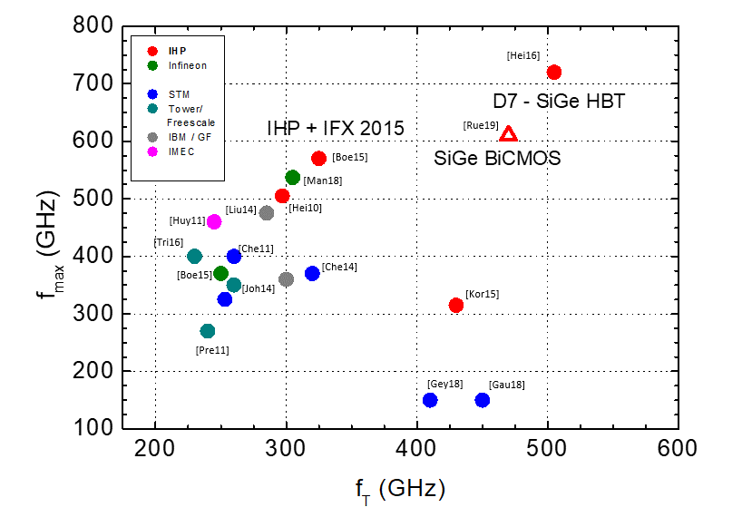
World's Fastest SiGe-based THz Transistors in CMOS

Representation of the cut-off frequency as a function of the maximum frequency - Illustration of the published performance data of SiGe heterobipolar transistors. With its SiGe-BiCMOS technology IHP represents the best-in-class technology.
© IHP
Representation of the cut-off frequency as a function of the maximum frequency - Illustration of the published performance data of SiGe heterobipolar transistors. With its SiGe-BiCMOS technology IHP represents the best-in-class technology.
  • New process options for vertical scaling of heterobipolar transistors (HBT)
  • Realization of HBT with cut-off frequencies > 0.6 THz in BiCMOS

Cooperations: 

Publications:

  • Rücker, H. et al. (2018): High-Performance SiGe HBTs for Next Generation BiCMOS Technology, Semicond, Sci. Technol., vol. 33, p. 114003 (2018). doi: 10.1088/1361-6641/aade64
  • Wolansky, D. et al. (2018): Impact of nickel silicide formations on SiGe BiCMOS devices, Semicond. Sci. Technol., vol. 33, p. 124003 (2018). doi: 10.1088/1361-6641/aae612
  • H. Rücker & B. Heinemann (2019): Device Architectures for High-Speed SiGe HBTs, 2019 IEEE BiCMOS and Compound semiconductor Integrated Circuits and Technology Symposium (BCICTS). doi: 10.1109/BCICTS45179.2019.8972757

Further information: 

Emerging Devices & Technologies