The technology platform MEMS Actuators focuses on design, materials and processes, system integration as well as characterization of materials, the test of devices and reliability assessments.
 

Design (analog and mixed signal design, designs for reliability, functional safety and harsh environments)

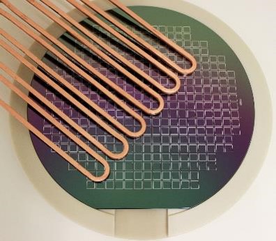
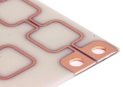
Material and Process Development for bulk and surface micromachining, including epitaxy, advanced Si Etch and piezoelectrical materials

Development of Devices like optical scanners, spatial light modulators (SLM) and acoustic actuators

Advanced Packaging and Silicon Micro Patterning and Methods of MEMS/NEMS Packaging e.g. hermetic glass packaging, wafer level capping can be offered as mature device technologies.

Test and Characterization of materials and devices (also in harsh environments); Nondestructive Analysis of Materials is widely possible in excellent quality; Device Degradation can be assessed, hetero-integrated systems can be characterized

Reliability Tests are feasible under multiple stress scenarios. Reliability Analysis under different loading is existing

MEMS actuators along the value chain

Flyer MEMS Actuators

Download Flyer


MEMS Micropump – TUDOS

Once a cancer tumor begins to metastasize, the chances of recovery diminish significantly. Fraunhofer EMFT tackled the challenge in the project μP Brain Test.


MEMS/CMOS Integration

In a well-established, highly productive cooperation, the Fraunhofer institutes IMS and IPMS are developing a process for integrating actuators on CMOS backplanes.

Scientific excellency in MEMS Actuators

With its 13 member institutes of the Fraunhofer-Gesellschaft and Leibniz Association, the Research Fab Microelectronics Germany (FMD) demonstrates research achievements of international excellence. In this way, FMD contributes to Germany and Europe, taking a leading position in research and development. Some selected research highlights and lighthouse projects in the field of MEMS actuators can be found below.

Selective low-temperature bonding - reactive bonding

Mittels CuO/Al oxidbasierter reaktiver Multilagen gefügter Silizium-Glas Waferverbund und gesputterter Multilagenstapel
© Fraunhofer ENAS
Mittels CuO/Al oxidbasierter reaktiver Multilagen gefügter Silizium-Glas Waferverbund und gesputterter Multilagenstapel
  • Low temperature joining process for integration of heterogeneous wafers, chips and components based on self-propagating exothermic reactions
  • selective heat input from the interlayer itself
  • high propagation (>1m/s) and very high joining speed ( < 1s)
  • structured integrated layers on chip and wafer level
  • adapted material systems for different applications (CuO/Al, Pd/Al)
  • worldwide first ECD iRMS for direct deposition on printed circuit boards and ceramic substrates (Pd/Sn)

Cooperation:

AiF / IGF-Projekt reMMi
 

Publications:

  • Hertel S, et al. (2020): Electroplating of Pd/Sn Multilayers for Reactive Bonding in Packaging and Assembly Applications, in 2020 IEEE 8th Electronics System-Integration Technology Conference (ESTC). doi: 10.1109/ESTC48849.2020.9229651)
  • Wiemer M, et al.(2020): Selective Heat Input for Low Temperature Metallic Wafer Level Bonding, in 2020 ECS Trans. 98 183. doi: 10.1149/09804.0183ecst)
  • Vogel K, et al.(2021): Reactive Bonding, in 3D and Circuit Integration of MEMS chapter 14. doi: 10.1002/9783527823239.ch14

Further information: 

ENAS research focus: wafer-to-wafer bonding / reactive bonding

Selective low temperature bonding - inductive wafer bonding

© Fraunhofer ENAS
Größenvergleich: Kupfer-Makrospule und Bondrahmen
© Fraunhofer ENAS
Kupfer-Mikrospule mit Kontaktpads
  • novel waferbond technology for the packaging of microsystem technology systems with metallic interlayers
  • selective, very fast (∆T > 100 K/s) and energy-efficient heat input into the metallic joining/intermediate layer
  • worldwide first use of planar microcoils (Cu-ECD, < 500 µm) for induction heating (previous coils: copper profile tubes > 2 mm)
  • Use of induction generators (f ≈ 2 MHz) and plasma generators (f ≈ 40 MHz) for inductive energy supply

Cooperations:

  • ZIM cooperation network SCALE
  • AiF / IGF projects InduBond and GeoTech
  • AiF / ZIM projects Indu2Mikro and UHF-Bond

Publications:

  • Hofmann C, et al (2019): A Novel Method for MEMS Wafer-Level Packaging: Selective and Rapid Induction Heating for Copper-Tin SLID Bonding, in 2019 20th International Conference on Solid-State Sensors, Actuators and Microsystems & Eurosensors XXXIII (TRANSDUCERS & EUROSENSORS XXXIII). doi: 10.1109/TRANSDUCERS.2019.8808256
  • Hofmann C, et al.: Verfahren zum Erwärmen einer Vielzahl von elektrisch leitfähigen Strukturen sowie Vorrichtung zur Verwendung in dem Verfahren (Patentnummer: 10 2019 206 248 A1)
  • Wiemer M, et al.(2020): Selective Heat Input for Low Temperature Metallic Wafer Level Bonding, in 2020 ECS Trans. 98 183. doi: 10.1149/09804.0183ecst

Further information: 

www.scale-netzwerk.de

Piezoelectrically Actuated Micromirrors

Built-up micro mirrors with piezoelectric AlN as transducer material.
© Fraunhofer ENAS
Built-up micro mirrors with piezoelectric AlN as transducer material.

World's first micro mirror with piezoelectric AlN as transducer material, which can realize a deflection angle of up to 25° (previous concepts create angles of 2-4°).

Cooperations:

  • AiF Project PI MEMS Control
  • SAB Junior Research Group E-PISA

Publications:

  • Meinel K, et.al. (2019): Piezoelectric Scanning Micromirror with Large Scan Angle Based on Thin Film Aluminum Nitride, in 20th International Conference on Solid-State Sensors, Actuators and Microsystems & Eurosensors XXXIII (TRANSDUCERS & EUROSENSORS XXXIII), Germany, 2019, pp. 1518-1521. doi: 10.1109/TRANSDUCERS.2019.8808723
  • Meinel K, et.al. (2020): Piezoelectric scanning micromirror with built-in sensors based on thin film aluminum nitride, in IEEE Sensors Journal, early access. doi: 10.1109/JSEN.2020.2997873
  • Meinel K, et.al. (2019): Piezoelectric scanning micromirror with built-in sensors based on thin film aluminum nitride, in IEEE SENSORS, Canada, 2019, pp. 1-4. doi: 10.1109/SENSORS43011.2019.8956929

Further information: 

Piezoelectric Micro Sensors based on aluminum nitride

Photonic Microsystems - MEMS-on-CMOS

Micro mirror array
© Fraunhofer IPMS
Micro mirror array
  • >>1 million individually controllable single mirrors with high integration density and pixel sizes down to 4 µm (worldwide unique)
  • Leading institute for the development of customer-specific, micro-mirror array-based surface light modulators (SLMs)
  • MEMS devices with analog/digital, tilt, and drop actuators or combined functionality
  • Surface micromechanics technology (MEMS-on-CMOS) with TiAl/USG as structural and sacrificial layers
  • Reduction of adhesive forces on MEMS contact surfaces implemented by the use of non-stick layers
  • Integrated CMOS drive circuit and external address electronics and data interface in continuous performance optimization
  • Goal: structural reduction through the use of DUV lithography and process control / metrology (e.g. coverage accuracy, OVL) for use in holography and other applications
  • Patented technology: US7424330, US 8531755, DE201510200626, DE102018215428

Cooperations:

EU-funded project SURPRISE (H2020)

Publications: 

  • Gehner A, et al. (2020): Novel CMOS-integrated 512x320 tip-tilt micro mirror array and related technology platform, in MOEMS and Miniaturized Systems XIX, Proc. of SPIE Vol. 11293, 1129302 (2020). doi: 10.1117/12.2543052
  • Dürr P (2019): MEMS Piston Mirror Arrays with Force-Balanced Single Spring, in MOEMS and Miniaturized Systems XVIII, Proc. SPIE 10931, 1093104 (2019). doi: 10.1117/12.2507007

Further information: 

Smart Industrial Solutions

Aluminum ECD​

Aluminium Bumps mit 30 µm Durchmesser für die Ultraschall-FlipChip Montage (Abscheide und Bond derzeit in Entwicklung)
© Fraunhofer ENAS
Aluminium Bumps mit 30 µm Durchmesser für die Ultraschall-FlipChip Montage (Abscheide und Bond derzeit in Entwicklung)
  • Al electroplating from ionic liquids
  • Novel process control for Al electroplating of circuit boards, Si wafers or special substrates
  • Full area deposition and pattern plating
  • Viafilling and bump deposition
  • Equipment for WL substrates up to 6 inch available
  • Cooperation with group of companies for the development of industrial deposition equipments

Cooperations: 

  • AIF/ZIM: Alma, Adept​
  • BMBF supported procect Aioli 

Publications:

  • Al Farisi M, et al. (2018): Aluminum Patterned Electroplating from AlCl3-[EMIm]Cl Ionic Liquid Toward Microsystems Application, in Micromachines 2018, 9(11), 589. doi: 10.3390/mi9110589
  • Hertel S. et al. (2018): Electrochemical deposition of reactive material systems for assembly and packaging, in Micro-Nano-Integration; 7th GMM-Workshop. (ISBN 978-3-8007-4789-4)​
  • Hertel S, et al. (2018): Galvanische Aluminium-Abscheidung auf unerschiedlichen Startschichten für die Leiterplatten- und Mikrosystemtechnik, in Jahrbuch Oberflächentechnik Band 74. (ISBN 978-3-87480-349-6)​

Further information: 

Research Field Electrochemical Deposition @ Fraunhofer ENAS

MEMS Loudspeakers for Mobile Applications

In-ear headphones with integrated MEMS speakers.
© Fraunhofer ISIT
In-ear headphones with integrated MEMS speakers.
  • The world's most powerful integrated MEMS loudspeaker technology
  • High playback quality, small size, and high efficiency
  • Drive via sputtered piezoelectric thin films

Cooperations: 

Publications:

  • Männchen A, et. al. (2019): Design and electroacoustic analysis of a piezoelectric MEMS in-ear headphone, in Audio Engineering Society Conference on Headphone Technology, 2019 USA. Online abrufbar unter: http://publica.fraunhofer.de/documents/N-564755.html
  • Stoppel F, et al. (2018): New integrated full-range MEMS speaker for in-ear applications, in 2018 IEEE Micro Electro Mechanical Systems (MEMS), 2018, pp. 1068–1071. doi 10.1109/MEMSYS.2018.8346744
  • Stoppel F, et al. (2017): Novel type of MEMS loudspeaker featuring membrane-less two-way sound generation, in Audio Engineering Society, Convention Paper, 143rd Convention 2017 USA. Online available at: http://publica.fraunhofer.de/dokumente/N-518560.html

Further Information: 

Acoustic Systems and Micro Actuators