Multi Project Technologies

Multi Project Technologies (MPT) are giving an extended group of customers access to specific standardized process steps that can be therefore made available for the customers own projects. This implies a high Technology Readiness Level of at least TRL ≥ 7.

High cost reduction potential

Due to the versatile application possibilites of these technologies, a cost reduction for the end customer is very common, as production start-up costs can be reduced significantly through the use of MPTs.

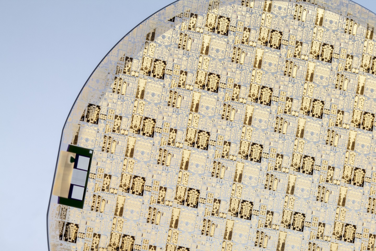
Further financial advantage through multi-project wafers (MPW)

Multi-project wafers (also multi-purpose wafers) can create a further financial advantage. Usually the costs for lithography mask sets are very high; though they can be shared through MPWs. In this case, the interested customers own design can be placed on the reticle. This leads to a cost reduction of up to 90 % compared to an own development process without a partner.
 

MPW Runs are especially beneficial in the following scenarios:

  • Product Prototyping,
  • IP verification, design libraries,
  • Device characterization,
  • Low volume manufacturing,
  • "Proof of concept" for research and development projects,
  • Experiments with new circuits/ First Silicon verification.

In addition, this service helps you to get to market faster ("Time to Market").

FMDs MPT-Services

The FMD member institutes are offering a variety of MPT-services, either through external service providers or on their own. Here you can find a list of the service spectrum.

Europractice

A European provider that organizes and assembles MPW Runs (or "Silicon Shuttles") is EUROPRACTICE. The organization was founded by the EU in 1995 as a successor to Eurochip. In the consortium the following tasks are secured: Design tools, training, prototyping, system integration and small volume production for industry and research. Prototyping and small volume production are ensured for four areas: ASICs (application-specific-integrated-circuits), MEMS, photonics and smart power.

Leibniz IHP

SiGe-BiCMOS Technologies & Modules (0.25µm, 0.13µm)

Fraunhofer IZM

Multi-Project Fan-Out Wafer Level Packaging (MPFOWLP) Technologies

Fraunhofer IIS

ASIC Foundry Services

JePPIX

Jeppix offers specialized MPW runs, pilot line services and trainings for photonics.

Fraunhofer HHI

InP-Platform for Multi-Project Wafer Runs

FMD's in-house technology services

Within the FMD, we are also enabling our excellent technology competencies to external partners from industry and academia without a separate service provider. This includes offers from the areas of epitaxy, MEMS, screening platform, organic field effect transistors, backend technologies, and the π-Fab - prototype services for electronic components.

Epitaxy

Fraunhofer IAF

Customer-specific epitaxial layers

as well as: High frequency circuits and modules based on InGaAs mHEMT and GaN technologies

Leibniz FBH

Customer-specific epitaxial layers

based on GaAs and InP as well as GaN

MEMS

Fraunhofer IPMS

200 mm MEMS Foundry Services

Screening Plattform

Fraunhofer IPMS

Screening Platform für processes, materials and equipments on 300 mm Wafer

Organic field effect transistors

Fraunhofer IPMS

Organic field effect transistors (OFET)

Backend technologies

Fraunhofer IZM-ASSID

Test chip design with high density interconnects

π-Fab - Prototype services for electronic components

Fraunhofer IISB

Individual prototype services

as well as a continuous silicon-CMOS- as well as silicon-carbide production line in an industry-compliant environment. (Si, GaN, SiC)

Fraunhofer IISB

Focus on SiC services

III-V-based Multi Project Wafer Runs

Fraunhofer IAF

Multi-Project Wafer Runs

and dedicated wafer runs for transistors and integrated circuits (ICs)