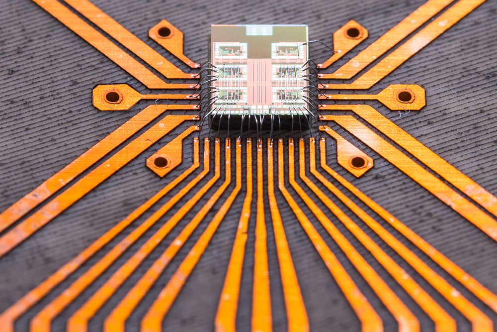
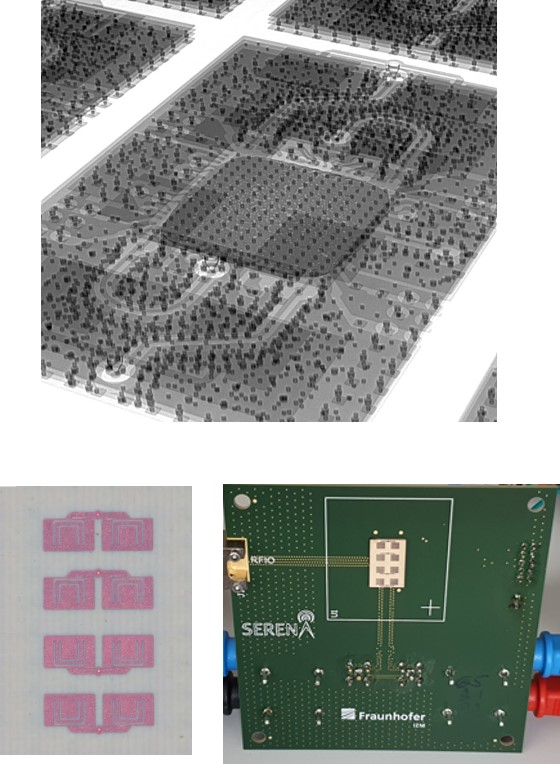
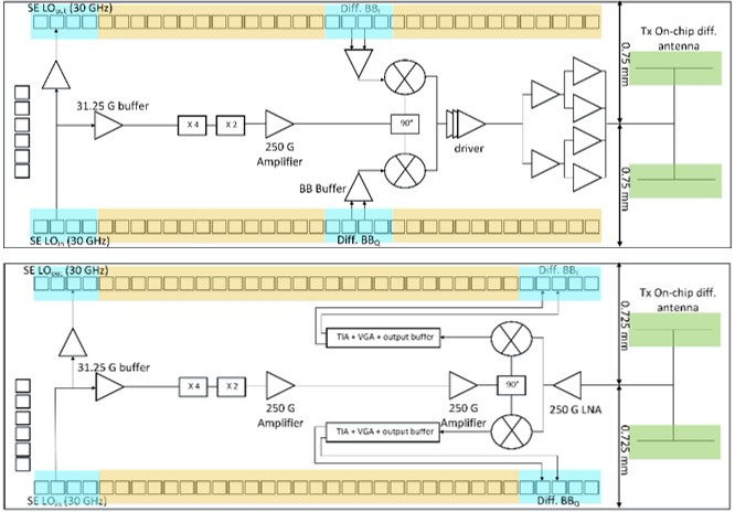
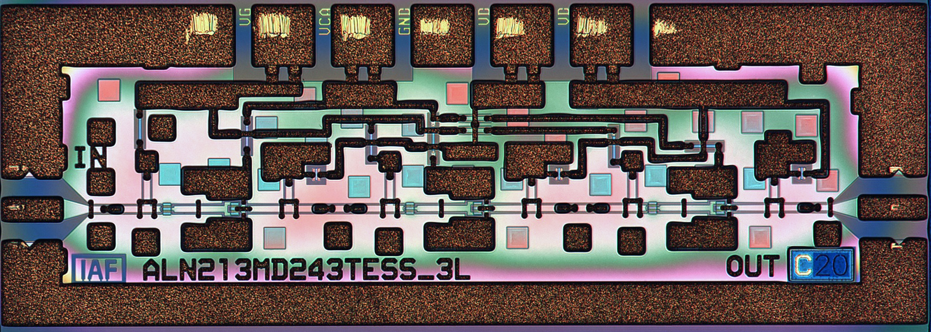
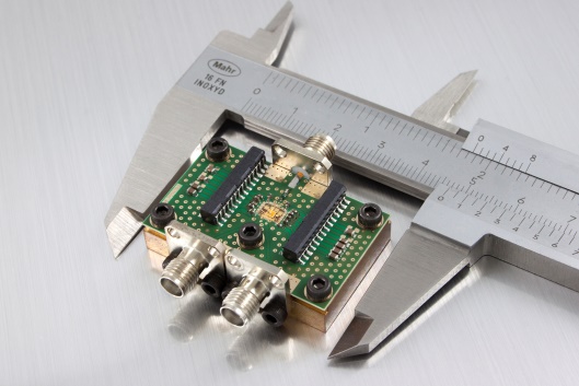
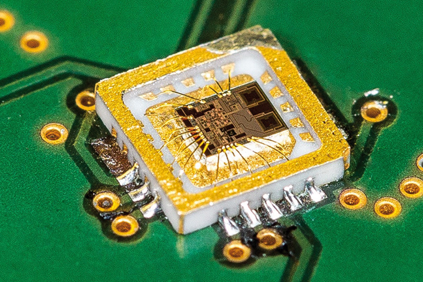
The technology platform Microwave & Terahertz offers turnkey as well as customized solutions along the entire microelectronic value chain. We can help you with profound knowledge in design, manufacturing, packaging and characterization, as well as cost-efficiency-tests for reliable devices with high performances, integrated circuits and systems for applications up to the THz-regime. In the development-section we focus on emerging future applications, especially the ones related to communication and sensing (e.g. 5G mm-Wave or radar sensing for autonomous / self-driving vehicles).
In-depth knowledge in Packaging and Heterointegration for high frequency applications
Leading-edge Devices and Circuits for applications up to the THz-regime
Design of Systems e.g. for communication or high and ultra-high frequencies
FMD offers Si-based and Compound-Semiconductor-based Cleanrooms that allow processing of Si, SiGe, InP, GaN/SiC, InGaAs/GaAs to build devices such as HBTs, HEMTs, passive structures or mm-Wave Integrated Circuits (MMICs)
R&D on the Integration of III-V-materials into Si-based Technologies
Integration of InP-based HBT BICMOS Technology into one single chip
Test and Characterization of designed, with SiGe:C manufactured and assembled systems (also in harsh environments)
Europractice IC Service: Multi Project Wafer (MPW) and Prototyping
Within the EUROPRACTICE IC Service, the Leibniz IHP as part of the Research Fab Microelectronics Germany, is providing a manufacturing service for Multi Project Wafer (MPW) and Prototyping. More information here.
 Fraunhofer Group for Microelectronics in cooperation with the Leibniz institutes IHP and FBH