CAM workshop: New approaches for failure analysis and material diagnostics of electronic components
Efficient failure analysis is essential for high-performance electronic applications and the development of cutting-edge solutions for the European semiconductor industry. This was the conclusion of the CAM workshop at the Fraunhofer Institute for Microstructure of Materials and Systems IMWS in Halle (Saale) yesterday. More than 150 international guests learned about possible applications for gallium nitride (GaN) and the pilot line for Advanced Packaging and Integration for Electronic Components and Systems (APECS).

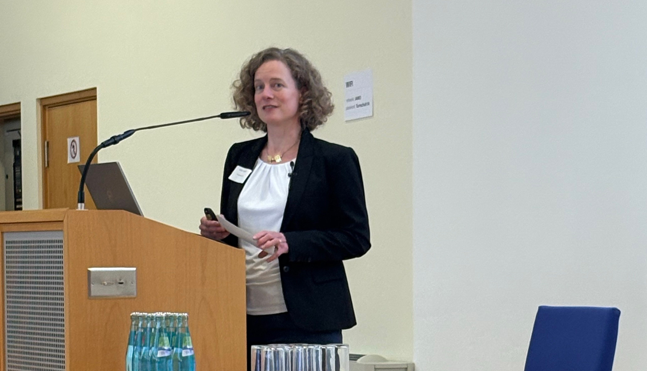
"We succeeded in establishing our CAM workshop as an important international platform for questions relating to quality assurance and failure analysis in electronics. I am very pleased that we were able to welcome so many top-class guests again this year and show how important the exchange of information on new analysis tools, technological challenges and methodological approaches for defect detection and material characterization is," says Frank Altmann, head of the "Materials and Components for Electronics" business unit at the Fraunhofer IMWS.
The conference focused on new results in defect localization and analysis, case studies on troubleshooting workflows and innovations in material characterization. Particular attention was paid to MEMS (Micro-Electro-Mechanical Systems) sensors and gallium nitride (GaN)-based power semiconductors.
In an exciting keynote speech, Thomas Detzel (Infineon Austria) presented the advantages of GaN power devices and systems as well as their industrial realization in a variety of applications. Mikel Azpeitia Urquia (STMicroelectronics, Italy) addressed the importance of MEMS-based sensors as a key technology for energy-efficient AI applications. Konstantin Schekotihin (University of Klagenfurt) presented the current state of research on AI applications in failure analysis laboratories. Ingrid de Wolf (imec, Belgium) rounded off the program with a tutorial on the role of mechanical stress in microelectronics and its impact on reliability.
One highlight was the presentation by Ulrike Ganesh (Fraunhofer Institute for Reliability and Microintegration IZM) on the APECS pilot line, which is being created as a European innovation platform for chiplet technologies as part of the EU Chips Act. Ganesh impressively explained how the industry is supported here by the provision of a versatile technology portfolio for the further development of packaging technologies and heterogeneous integration. These technologies are of crucial importance for applications such as telecommunications, artificial intelligence and medical instruments. The combined expertise of ten partners of the Research Fab Microelectronics Germany (FMD) in APECS opens up unique opportunities for seamless design-to-production capabilities and scalable manufacturing solutions for the electronics industry.
The Fraunhofer IMWS is playing a decisive role in setting up the APECS pilot line and is contributing in particular with its expertise in precise defect detection, high-resolution microstructure analysis, local characteristic value determination and reliability analyses, including the investigation of novel failure mechanisms of functionally complex electronic components. "The systematic inclusion of characterization, testing and reliability issues in technology development is a key factor for high production quality, long service life and the rapid market launch of new, particularly highly complex heterointegrated components. We are very proud to be able to contribute our internationally recognized expertise in the field of reliability research and failure analysis to the APECS pilot line," says Altmann.
The program of the CAM workshop included three current contributions from the institute. Sebastian Brand presented new approaches for the precise 3D-resolution localization of electrical defects in 3D-integrated components through quantitative analysis of heat propagation using lock-in thermography. Michél Simon-Najasek presented a new approach for combined planar and cross-sectional analysis of gate defects in electrically stressed normally-on HEMT devices. Lorenz Heinemann explained how machine-learning-based acoustic signal analysis for the automated detection of delamination and crack defects can be simplified using device-independent transfer functions.
For the twelfth time, the CAM workshop in Halle (Saale) brought together international experts from the electronics industry as well as manufacturers of analysis equipment and research institutions to discuss challenges, future requirements and innovative solutions in defect diagnostics and material characterization. In addition to the numerous specialist presentations from the industry, the high level of application relevance was also underpinned by an accompanying industrial equipment exhibition.
The images may be used free of charge for editorial purposes for reporting on this topic. Use for other purposes is only permitted with the prior consent of the Fraunhofer IMWS.
About the Fraunhofer Institute for Microstructure of Materials and Systems IMWS
The Fraunhofer Institute for Microstructure of Materials and Systems IMWS in Halle (Saale) offers microstructure-based diagnostics and technology development for innovative materials, components and systems. Building on its core competencies in high-performance microstructure analysis and microstructure-based material design, the institute researches questions of functionality and application behavior as well as the reliability, safety and service life of materials that are used in various market and business areas with high significance for social and economic development. For its partners in industry and for public clients, the Fraunhofer IMWS pursues the goal of contributing to the accelerated development of new materials, increasing material efficiency and cost-effectiveness and conserving resources. In this way, the institute contributes to securing the innovative capacity of important future fields and to sustainability as a central challenge of the 21st century.
About the pilot line for Advanced Packaging and Integration for Electronic Components and Systems (APECS)
As part of the EU Chips Act, the Research Fab Microelectronics Germany (FMD) will establish a comprehensive pilot line for resilient and trustworthy heterogeneous systems with APECS in the coming years, which will promote the innovative capacity of European industry across the board and form an essential building block with regard to Europe's technological resilience. By enabling new functionalities through System Technology Co-Optimization (STCO), end-to-end design and pilot production capabilities, the pilot line will enable innovation to evolve from research to practical, scalable manufacturing solutions. In addition, APECS offers a one-stop store for customers in virtually all traditional industry verticals, including large enterprises, SMEs and start-ups. APECS brings together the expertise, infrastructure and know-how of ten partners from eight European countries. In Germany, twelve institutes of the Fraunhofer-Gesellschaft (project coordinator) and two institutes of the Leibniz Association are involved in the pilot line. APECS is managed by FMD - one of the world's leading cross-location R&D consortia for micro- and nanoelectronics.
About the Research Fab Microelectronics Germany
As a cooperation of the Fraunhofer Group for Microelectronics with the Leibniz institutes FBH and IHP, the Research Fab Microelectronics Germany (Forschungsfabrik Mikroelektronik Deutschland FMD) is the central contact for all matters concerning micro- and nanoelectronics. As a one-stop shop, FMD has been combining scientific excellence, application-oriented technologies and system solutions of the 15 cooperating institutes from the Fraunhofer-Gesellschaft and Leibniz Association into a broad customer-tailored technology portfolio since 2017. The cooperating institutes of FMD are: Fraunhofer AISEC, EMFT, ENAS, FHR, HHI, IAF, IIS, IISB, IMS, IMWS, ISIT, IPMS, IZM and Leibniz FBH, IHP. For more information, please visit: www.forschungsfabrik-mikroelektronik.de/en
Last modified: