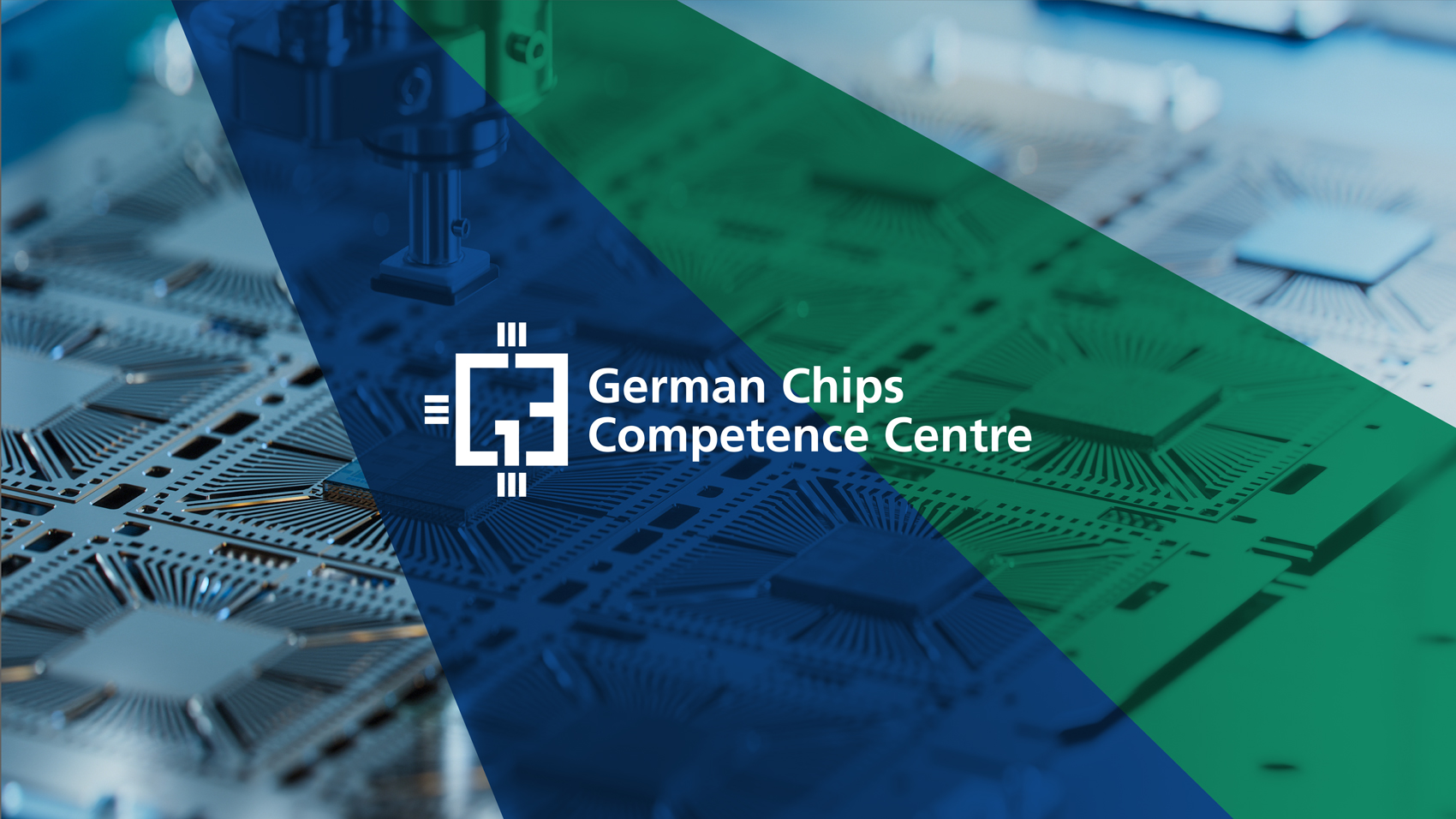
German Chips Competence Centre launched as gateway to European pilot lines and design infrastructure
With the launch of the German Chips Competence Centre (G3C), companies and research institutions in Germany gain direct access to Europe's most advanced semiconductor infra-structure. Serving as a central gateway, the G3C links Germany’s semiconductor ecosystem with European design and manufacturing pilot lines, coordinates their use, and facilitates collaboration across EU member states. This allows German players to benefit earlier from the latest innovations, boosting Germany's position as a leading semiconductor hub beyond its borders. Over the next four years, the G3C will be established by the Research Fab Microelectronics Germany (FMD). It is funded by the European Union under the EU Chips Act, with additional national co-funding from the Fed-eral Ministry of Education and Research (BMFTR).

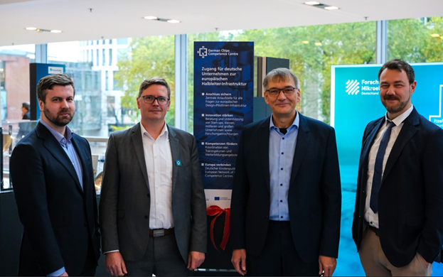
On October 28, 2025, the German Chips Competence Centre (G3C) was officially unveiled at the MicroSystem Technology Congress in Duisburg, featuring contributions from Dr. Stephan Guttowski (Managing Director of the FMD Business Office), Dr. Oliver Höing (Advisor at the BMFTR), Alexander Stanitzki (G3C project manager), and Dr. Björn Lekitsch (co-founder and CTO of neQxt).
At the heart of the EU Chips Act is the creation of Chips Competence Centres across Europe, complementing the development of European pilot lines. Together, they form the backbone of Europe’s effort to bring research and industry closer together. The G3C serves as Germany’s access point within this pan-European network, strengthening Europe’s competitiveness and innovation potential.
“Europe is now shaping the future of its semiconductor industry. With the G3C, Germany demonstrates its expertise and promotes German know-how and technology transfer across Europe”, asserts Matthias Hauer, Parliamentary State Secretary at the BMFTR.
Enabling access for companies, research institutions, and start-ups
The G3C supports Germany-based start-ups, SMEs, and established companies in accessing Europe’s design and pilot-line infrastructure for key technologies such as advanced packaging, photonic integrated circuits, FD-SOI, and wide-bandgap semiconductors. It aims is to lower innovation barriers and speeds up market entry, particularly for companies with limited access to complex development and testing en
“With the G3C, we are building a bridge between Germany’s innovation community and Europe’s chip infrastructure, spanning both chip design and manufacturing. For SMEs and start-ups especially, this means easier prototyping, faster scaling from lab to series production, and earlier market access. The G3C thereby strengthens their prospects for success in global markets. Looking ahead, the introduction of hands-on training and further education initiatives will help develop the expertise urgently needed across the semiconductor sector,” explains Alexander Stanitzki, G3C project manager.”
Acting as Germany’s national gateway, the G3C brings together information across the full range of European design and manufacturing opportunities, offers guidance on their use, and coordinates training and continuing education programs. It serves as coordination figure, aligned with other European Chips Competence Centres, ensuring that relevant infrastructure and services are accessible across national borders.
“For start-ups like ours, the G3C represents significant added value,” affirms Dr. Björn Lekitsch, co-founder and CTO of neQxt. “We hope the Chips Competence Centre will give us access to resources and enable easier, more effective networking with key technology partners, helping us accelerate our development projects. For neQxt, this strengthens our competitive position and supports an earlier market entry for our upcoming product portfolio.”
Raising visibility and deepening coordination in Europe
The G3C, launched under the EU Chips Act, strengthens Europe’s technological resilience and supports the growth of a competitive semiconductor industry. Alongside technological support, it serves a strategic liaison role by representing the German semiconductor ecosystem at the European level, ensuring international visibility, and contributing national expertise to the European Network of Chips Competence Centres (ENCCC).
“A key part of the mission is close cooperation with established structures such as the APECS pilot line,” explains Dr. Stephan Guttowski, Head of the FMD Business Office, adding: “the G3C also connecs with other pilot lines – FAMES, NanoIC, PIXEurope, and WBG – to foster synergies across the entire microelectronics value chain.”
The G3C thus creates an end-to-end system providing industry with access to everything it needs for innovation.
Boosting Germany as a semiconductor hub
Thanks to the G3C, Germany now has centralized access to Europe’s most advanced semiconductor infrastructure. By pooling knowledge, fostering partnerships, and opening new paths for research and innovation, the G3C strengthens Germany’s innovation potential, competitiveness, and international visibility as a semiconductor hub.
The G3C is funded with €7.9 million over a four-year project period.
![Press picture 1 [ PNG 0.53 MB ]](/content/dam/ipms/forschungsfabrik-mikroelektronik/de/Pressemitteilungen/folder-2025/g3c-pm.png)
![Keyvisual G3C [ JPG 0.69 MB ]](/content/dam/ipms/forschungsfabrik-mikroelektronik/de/Pressemitteilungen/folder-2025/fmd_g3c_keyvisual.jpg)
Last modified: