Sensors and Sensor Systems
Machine Close-up: 12" thin wire bonder and X-ray photoelectron spectrometer
215 newly installed machines in 2019: As part of the Research Fab Microelectronics Germany‘s (FMD) investments, the 13 member institutes are expanding and modernizing their infrastructure. The following two examples illustrate the institutes’ new competencies gained by this.
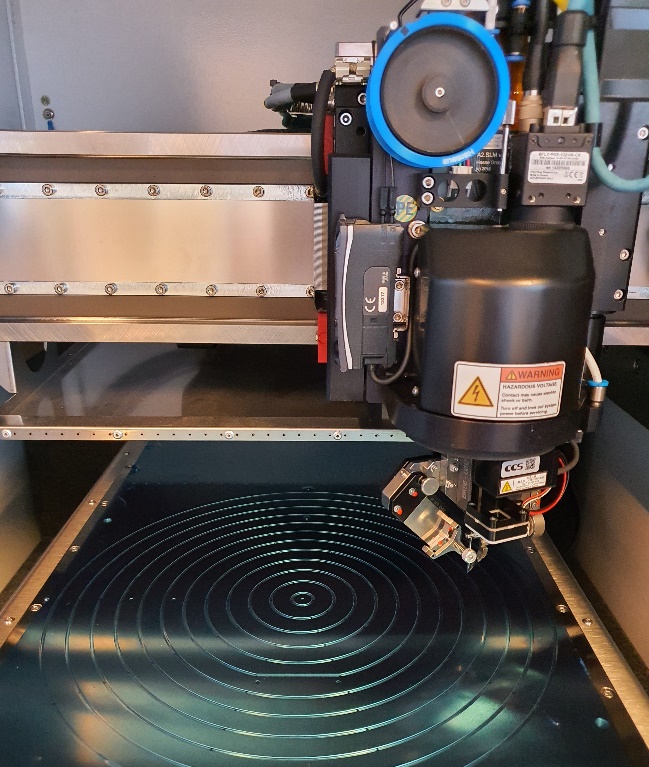
Fully automatic: 12" thin wire bonder at Fraunhofer ISIT
The newly installed thin wire bonder Bondjet 855 of the company Hesse mechatronics was modified according to the requirements of the employees of the working group "Module Services" at Fraunhofer ISIT. The software and also the specific innovations are very different from the predecessing model. Different bond heads can now be mounted on the new device, which are optimized for the respective task. Thanks to the high performance, up to seven bond connections per second can be realized. In addition, it is possible to suck in wafers of up to 12" in size using vacuum, to heat them and to process them completely.
The machine has three working areas which automatically detect the wafer size and switch the vacuum separately. Each wafer size is thus ready for programming and processing at the push of a button without any conversion. For boards, ceramics and individual components to be taught and bonded, the thin wire bonder also has a large, rectangular working area with suction holes. The distance between them is very small in order to hold the flat samples well. The table of the machine is heatable which allows a wide variety of wire and ribbon materials to be used, such as gold, copper, silver and platinum wires as well as aluminium and gold ribbons.
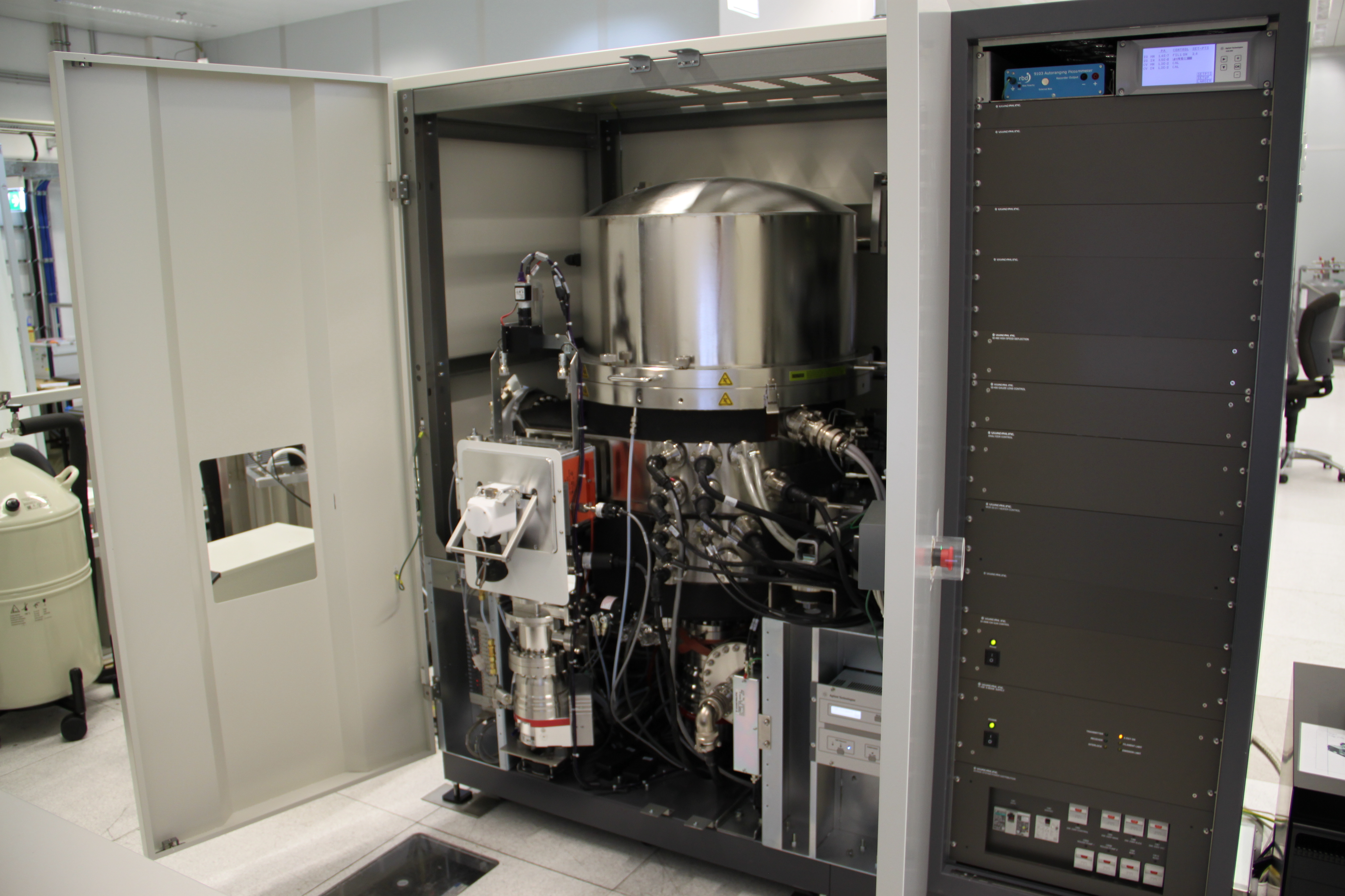
View into nano-depths: X-ray photoelectron spectrometer at Fraunhofer IPMS
Silicon chips are the nerve cells of artificial intelligence. Their surfaces contain billions of tiny components that transmit important information and signals. But the demands on semiconductor chips are increasing. Fraunhofer IPMS has acquired a new X-ray photoelectron spectrometer (XPS) from Physical Electronics GmbH as part of the FMD investments. The spectrometer is used to analyze the surfaces of silicon chips and to realize experiments in the nanoscale. Thus, surface features, thin-film structures and contaminations can be examined down to the nano range without damage. The investigation in this area is important to analyse the exact chemical composition of the chip surfaces. With this, processes for the production of semiconductor chips can be better understood and their later properties can be optimized.
A further advantage of the new acquisition is its versatility. In addition to conventional XPS measurements with an Al X-ray source, analysis experiments can be carried out with an extended depth. Moreover, thanks to the short-wave spectrum, transition metals can be analyzed and the system can be used for cleaning the sample surface and for depth profiling. In addition, the XPS allows temperature experiments from -120 °C to 300 °C and experiments with electrical sample contacting.
The project on which this publication is based was funded by Germany‘s Federal Ministry of Education and Research under the funding codes 16FMD01K, 16FMD02 and 16FMD03.
More informations here.
Last modified: