Examples for Europe's Only (and Internationally Recognized) 150 mm Research and Development Platform for 4H-SiC Components

Monolithically integrated load-break switch in JFET-based SiC technology

© Fraunhofer IISB
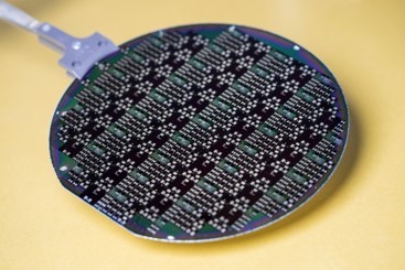
Complete 6'' SiC wafer with fabricated monolithic integrated load break switch devices.
© Fraunhofer IISB
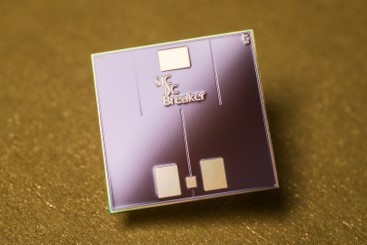
"SiC-DCBreaker" chip after the separation process.
© Fraunhofer IISB
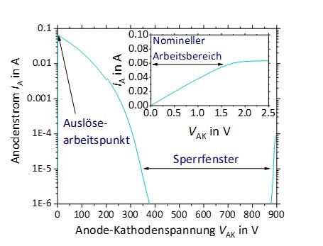
Measured output characteristic of a variant of the manufactured load-break switch components. The switch-disconnector carries the complete load current at all times. After the tripping current has been exceeded, the component immediately switches to blocking mode by itself. No external circuitry is required. The only requirement is that the DC link voltage is within the blocking window.
  • First monolithically integrated realization of the "dual thyristor" in 4H-SiC JFET technology with potential for high-volume manufacturing.
  • Self-powered, self-triggering and self-holding semiconductor-based fuse for DC grids and e-mobility applications
  • The engineered topology enables scalability of trip current and reverse voltage for application-specific requirements

Cooperations:

  • BMBF supported project „SiC-DCBreaker“03INT501BC
  • In-house research at the Fraunhofer IISB

Publications:

  • Boettcher N, Erlbacher T (2021): A Monolithically Integrated Circuit Breaker,  in IEEE Electron Device Letters ( Volume: 42, Issue: 10, Oct. 2021). doi: 0.1109/LED.2021.3102935.
  • Boettcher N, Erlbacher T (2020): Design Considerations on a Monolithically Integrated, Self Controlled and Regenerative 900 V SiC Circuit Breaker, in 2020 IEEE Workshop on Wide Bandgap Power Devices and Applications in Asia (WiPDA Asia). doi: 10.1109/WiPDAAsia49671.2020.9360279.
  • Huerner A, et al. (2017): Monolithically Integrated Solid-State-Circuit-Breaker for High Power Applications, in ICSCRM, Materials Science Forum Vol. 897, 2017. doi: 10.4028/www.scientific.net/msf.897.661

Further information:

#IISBinsights video

Lateral SiC power transistors in integrated circuits (SiC HV-CMOS technology)

© Fraunhofer IISB
Electric field strength in schematic cross section of lateral SiC power device for integrated circuits.
© Fraunhofer IISB
Results of the current-voltage measurement in the off-state.
© Fraunhofer IISB
Resistance in the forward state as a function of the breakdown voltage. The diagram shows the simulated values for different dosages of the RESURF layer.
  • Commercializable high voltage RESURF n-LDMOS transistor integrated into a high temperature (> 300°C) 1P2M 20V 4H-SiC CMOS technology.
  • Just one additional implantation step enables the insertion of a charge compensation layer into the LDMOS transistor, enabling a higher breakdown voltage.
  • Increased robustness of the transistor in the off-state while simultaneously reducing RON through a RESURF dose of 6*1012cm-2 and an implantation depth of 1 µm.
  • Modeling and simulation for mapping in the PDK

Cooperations:

  • DFG supported project "Charge compensation in 4H-SiC" ER 755/1-2.
  • ECSEL/BMBF supported project "IRel 4.0".
  • Industry and further research cooperations

Publication:

  • Weisse J, et al. (2020): RESURF n-LDMOS Transistor for Advanced Integrated Circuits in 4H-SiC, in IEEE Trans. Electron Dev. 67 (2020) 3278-3283. doi: 10.1109/TED.2020.3002730
  • Albrecht M et al. (2020): An Iterative Surface Potential Algorithm Including Interface Traps for Compact Modeling of SiC-MOSFETs, in IEEE Trans. Electron Dev. 67 (2020) 855-862. doi: 10.1109/TED.2020.2967507
  • Weisse J, et al. (2019): Aluminum acceptor activation and charge compensation in implanted p-type 4H-SiC, in AIP Advances 9 (2019) 055308. doi: 10.1063/1.5118666

Further information:

#IISBinsights video