Much of our work places the system center-stage as basic building block of functionality in microelectronics. System integration is necessary to translate technology advances on component level into enhanced functionality – but increasingly, integration involves system-level analysis and even further development or adaptation of existing system infrastructure.
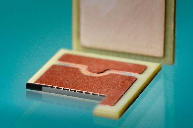
An example is the WBG semiconductor, whose superior switching performance, higher power density, and improved efficiency has caught the attention of early adopters and forward-thinking product designers looking for an edge on the market. However, not only has the new technology required integration on system level, the existing on-board packaging has had to be redesigned to meet the specifications of the semiconductor. We eliminated longstanding limitations in packaging design using the Bernstein module: a two-layer ceramic substrate with a cooler structure on the bottom, that yields extremely low DC link inductance, EMI shielding, a short thermal path, good heat spreading and mechanical stiffness against cooling water pressure. We also combine an innovative metalized transfer mold encapsulation with assembly of local DC link components as SMDs on top of the module. This close proximity of the SMD to the driver ensures fast switching and avoids parasitic switch-on. The result is a module with perfect switching at even the highest switching speed, high reliability, and lowest possible thermal resistance thanks to a low cost (plastic) cooler.