FIRST by FMD: Event Recap

A Successful Launch for FIRST by FMD: What Europe Needs for Faster Technology Transfer and a Resilient Semiconductor Industry

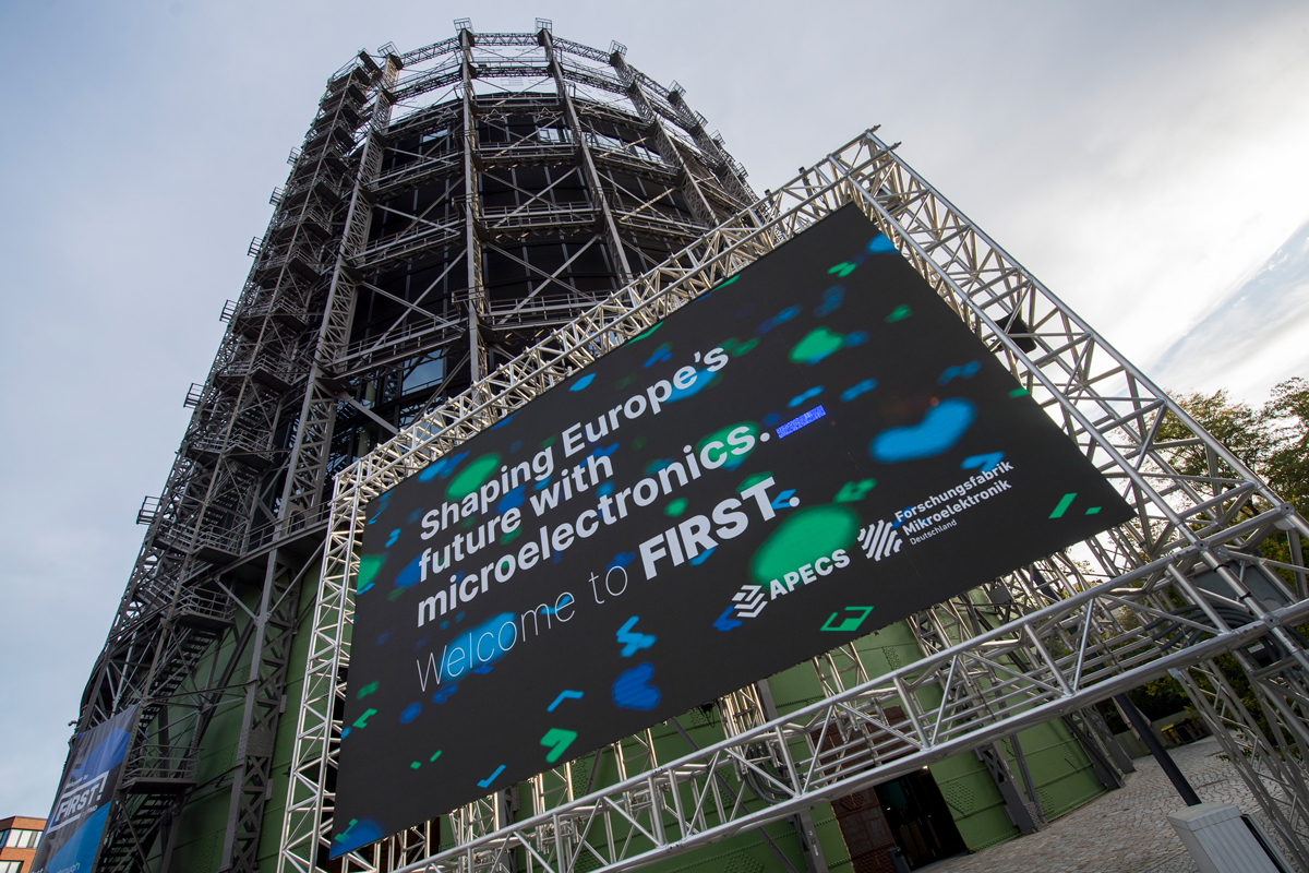
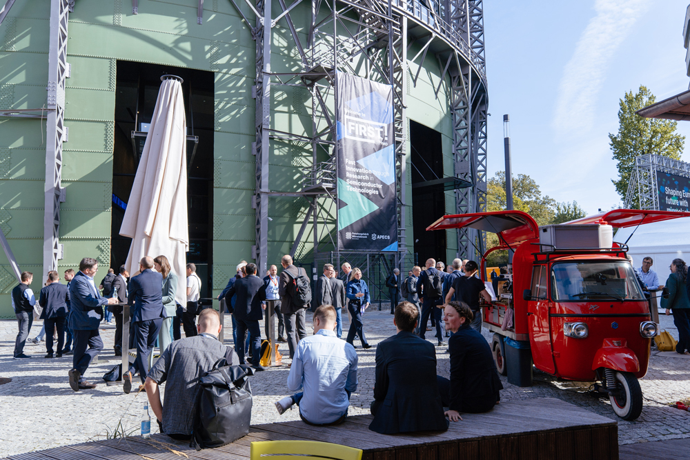
Over 550 industry, academic, and political decision-makers attended FIRST by FMD in Berlin to discuss the key prerequisites for Europe’s future through microelectronics, including faster technology transfer pathways, high-performance infrastructure, resilient value chains, and closer strategic coordination across national borders.

The overarching theme was »Shaping Europe’s future with semiconductors« and the central question was: How can Europe more quickly translate scientific excellence into scalable applications, competitive products, and lasting technological resilience?

FIRST by FMD was conceived by the Research Fab Microelectronics Germany (FMD) as part of the European APECS pilot initiative. It is a new European trend forum for microelectronics designed to bring together the industry’s key players. The event covered the following topics:

  • Current developments and industrial policy frameworks in the European semiconductor industry
  • European Chips Act, European roadmaps, and global competitive dynamics
  • Technological resilience, as well as production and scaling capabilities in Europe
  • Strategic collaborations along the microelectronics value chain.

FIRST stands for »Fast Innovation through Research in Semiconductor Technologies«. The name reflects the forum’s mission to accelerate the transition of new technologies into market-ready applications by bringing together research, infrastructure, and industrial needs. The FMD serves as a bridge between scientific excellence, industry-oriented development, and European collaboration in this process.

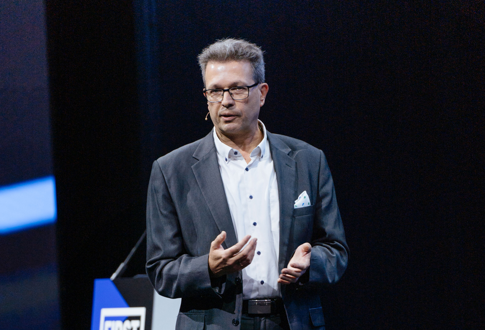
Prof. Dr. Holger Hanselka (President of Fraunhofer-Gesellschaft)

© Fraunhofer Mikroelektronik
Prof. Dr. Holger Hanselka (r.)

»Europe’s future in microelectronics will not be determined solely by roadmaps and work in laboratories, but by the joint commitment of industry and academia to rapidly translate research excellence into scalable industrial technologies.«

The Four Leverage Points for Europe's Semiconductor Future

Semiconductors as the Foundation of European Resilience

Semiconductors are the foundation of economic resilience, technological sovereignty, security, and sustainable growth. It depends on their availability whether Europe can independently shape future-oriented fields such as AI, mobility, energy, healthcare, and industrial manufacturing. FIRST by FMD addresses this strategic importance.  Therefore, the crucial question is not only which technologies Europe develops, but also how these can be quickly transformed into competitive products and robust value creation.

The EU Chips Act and Germany’s High-Tech Agenda establish important foundations for expanding European semiconductor expertise. However, investment alone is not enough; it must be combined with long-term technology roadmaps, appropriate technology transfer structures, and reliable conditions for industrial scaling.

Dr. Alexandra-Gwyn Paetz, from the Federal Ministry of Research, Technology and Space (BMFTR), highlighted Germany’s position in microelectronics.  FIRST by FMD brings these policy objectives into dialogue with technological developments and industrial roadmaps, discussing how to strengthen European value and supply chains.

Europe's resilience stems from the interplay of technology, infrastructure, industry, and politics. European investments can only lead to competitive products and resilient supply chains when research, technology transfer, scaling, and long-term value creation are planned together.

A Bridge to Industry: The APECS Pilot Line as a Catalyst

One of the key challenges for Europe’s semiconductor ecosystem is the gap between research results and industrial application. Discussions have revealed that innovations require accessible development environments, validatable processes, and scalable pathways. The APECS pilot line (Advanced Packaging and Heterogeneous Integration for Electronic Components and Systems) addresses this challenge.

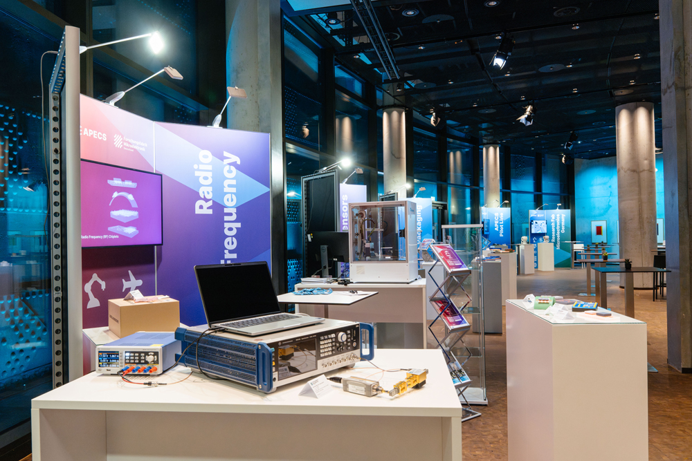
Led by the Fraunhofer-Gesellschaft and implemented by FMD, the APECS pilot line integrates design, development, testing, and industry-oriented processing. Companies and research institutions can further develop technologies for advanced packaging, heterogeneous integration, and chiplet architectures under real-world conditions. APECS thus builds a bridge between research excellence and industrial application.


How to Ensure Fast Transfers in Germany and Europe

Europe has outstanding research capabilities and enormous technological potential. To secure Europe’s future in microelectronics, it is crucial to translate this potential into industrial applications and value creation more quickly.

1. Access to industry-oriented pilot infrastructures — APECS enables the practical development and testing of chiplet, packaging, and integration solutions.

2. Early access to design capabilities — Shared design infrastructures, EDA tools, and AI-supported methods shorten the path to proof of concept.

3. Considering scalability from the outset — Processes, investments, supply chains, and production pathways must be planned together at an early stage.

4. Aligning roadmaps collectively — Research, industry, and policymakers should coordinate technological possibilities, market needs, and regulatory conditions early on.

Why Europe's Resilience Requires a Strong Microelectronics Sector

Technological resilience does not solely arise from increased manufacturing capacity. Europe must ensure that critical competencies remain available, interoperable, and industrially viable throughout the entire value chain — from design and manufacturing to packaging, testing, and reliability assessment.

  • Packaging and system integration as strategic competencies: With chiplets and heterointegration, a growing portion of system innovation is shifting to the packaging stage.
  • Trustworthiness as a development requirement: Security, traceable supply chains, and long-term availability must be considered from the initial design and system architecture stages.
  • Targeted autonomy rather than complete self-sufficiency: Europe should identify critical dependencies, expand strategic capabilities, and forge international partnerships based on its own strengths.

Dr. Dirk Schumann (FMD)

© Fraunhofer Mikroelektronik
Dr. Dirk Schumann (Research Fab Microelectronics Germany, FMD)

»FMD connects the required capabilities through one reliable partner across the innovation journey. Industrial R&D remains in the lead. But companies no longer have to build and manage the entire technology chain on their own. The result is clear: fewer interfaces, faster decisions and a shorter path from feasibility to an industrially usable solution.«

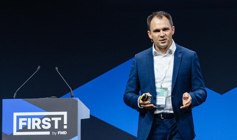
Marcel Schäfer (TRUMPF)

© Fraunhofer Mikroelektronik
Marcel Schäfer (TRUMPF)

»Advanced Packaging is the next battlefield. Europe needs packaging sovereignty alongside fab sovereignty. Laser beam-shaping enables chiplet integration at scale«

A Detailed Review of the Two-Day Conference; Poster downloads

Day 1 (September 30, 2026): Strategic Direction, Resilience, and the Europe 2035 Vision

© Fraunhofer Mikroelektronik
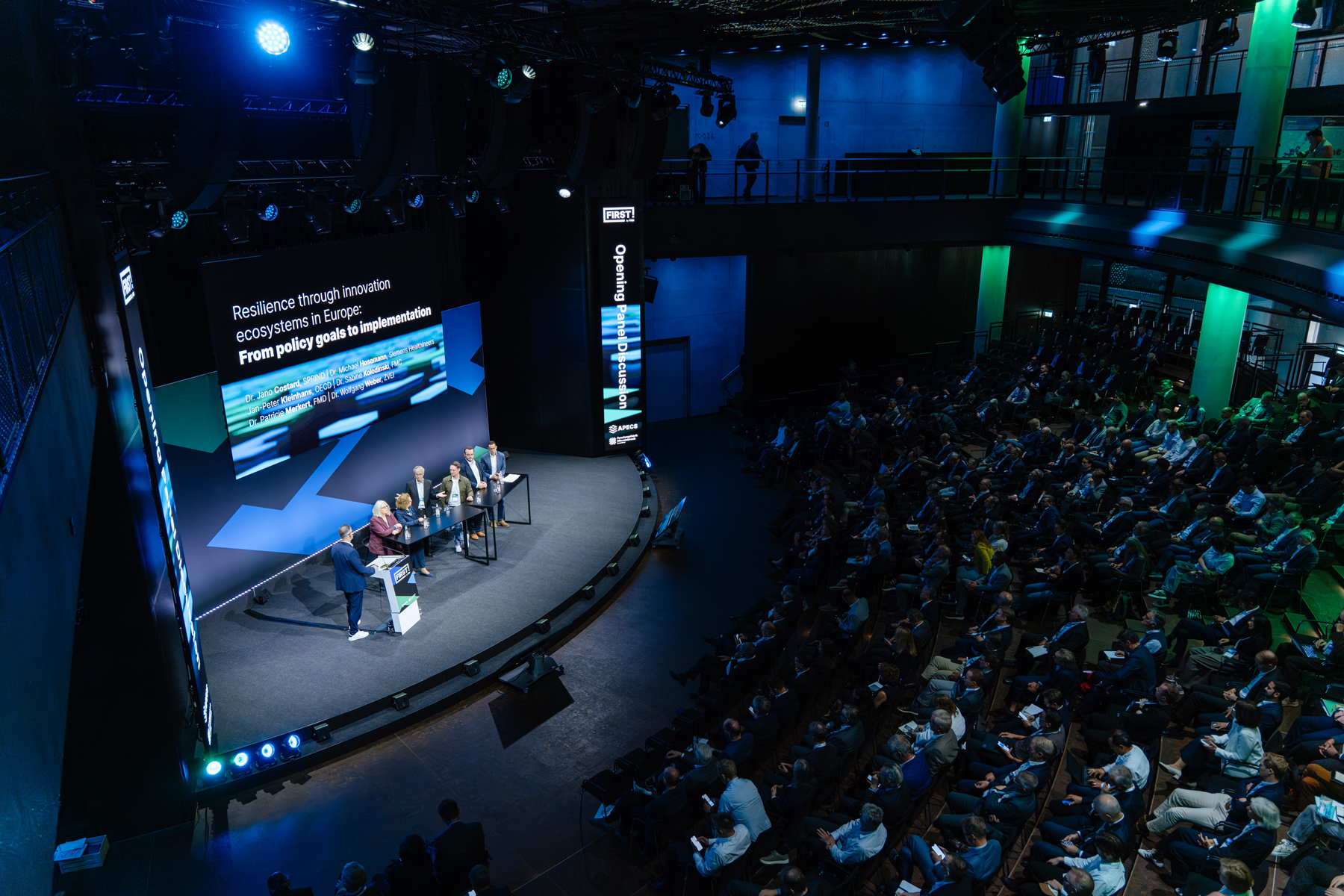
Opening panel discussion
© Fraunhofer Mikroelektronik
Dr. Alexandra-Gwyn Paetz (BMFTR)
© Fraunhofer Mikroelektronik
Panel discussion »Europe’s edge in microelectronics: From pilot lines to production – the vision Europe 2035«

Grand Opening & APECS Progress Showcase:

The event focused on technological trends and roadmaps, the EU Chips Act, the High-Tech Agenda Germany, and how Europe can strengthen its competitiveness and technological resilience. Speakers included Dr. Alexandra-Gwyn Paetz (BMFTR), Prof. Dr. Holger Hanselka (Fraunhofer-Gesellschaft), Prof. Dr. Albert Heuberger (Fraunhofer IIS/FMD), Dr. Manfred Horstmann (GlobalFoundries), and Dr. Dirk Schumann (FMD).

Opening Panel Discussion: Michael Hosemann (Siemens Healthineers), Jan-Peter Kleinhans (OECD), Dr. Sabine Kolodinski (FMC), Dr. Patricie Merkert (Fraunhofer IAF/FMD), and Dr. Wolfgang Weber (ZVEI) discussed securing value creation and strengthening technological leadership in European innovation ecosystems. The discussion focused on policy objectives, global developments, and the prerequisites for their practical implementation.

Session 1 »From Lab to Industry«: How can innovations be brought to market faster, and how can existing innovation gaps be closed? Engelbert Beyer (BMFTR), Sven Buchholz (ASMPT SMT Solutions), Dr. Christian Frank (SIKORA), Allan Frederiksen (Infineon Technologies), Ole Gerkensmeyer (Nexperia), and Prof. Dr. Axel Müller-Groeling (Fraunhofer Society) discussed strategies for overcoming the obstacles between research and industrial application and for increasing technological value creation in Europe.

Session 2 »Design-Infrastruktur & SiP-Workshop«: This session, featuring Prof. Dr. Amelie Hagelauer (Fraunhofer EMFT/FMD), Dr. Régis Hamelin (BLUMORPHO/ENCCC), Thomas Heurung (Siemens EDA), Dr. Benjamin Prautsch (Fraunhofer IIS/FMD), and Dr. Carlo Reita (Fondazione Chips-IT), focused on the role of European design infrastructures in promoting efficiency, innovation, and faster time-to-market. Meanwhile, the BMFTR workshop, »Shaping Europe’s SiP Ecosystem« drew on experiences from the »Tech for Trust« project and discussed the requirements for robust system-in-package infrastructures in Germany and Europe.

Vision Europe 2035: The first day concluded with the panel discussion, »Europe’s edge in microelectronics: From pilot lines to production – the vision Europe 2035«. Prof. Dr. Jens Eisert (Freie Universität Berlin), Fabio Gualandris (STMicroelectronics), Prof. Dr. Jari Kinaret (Chips Joint Undertaking), Carsten Salewski (Viscom SE/VDMA Productronic), and Dr. Andreas Werner (Rohde & Schwarz) discussed technological resilience, strategic partnerships, and production capacities. The discussion also focused on the prospects for the five European pilot lines and their role in Europe’s future innovation and production landscape.

Day 2 (October 1, 2026): APECS Pilot Line, Chiplets, and Technical Deep Dives

© Fraunhofer Mikroelektronik
Rolf Aschenbrenner (Fraunhofer IZM)
© Fraunhofer Mikroelektronik
Nikolaus Hahne (Quantune Technologies)
© Fraunhofer Mikroelektronik
Panel discussion »Beyond technology: Talent, skills, and sustainable workforce models for semiconductor excellence«

The second day focused on the industrial implementation and practical application of key European technologies. Under the theme of »APECS Pilot Line – European Chiplet Innovation« FIRST participants discussed how chiplet architectures, advanced packaging, and the expansion of European infrastructure are strengthening Europe’s technological resilience.

Session 3 »Microelectronics for tomorrow«: AI and quantum technologies were the focus of this session. Rolf Aschenbrenner (Fraunhofer IZM/FMD) and Hannes Voraberger (AT&S) discussed the new requirements in terms of integration, performance, and system architectures. They also addressed the role of advanced packaging and chiplet technologies in this context.

Session 4 »APECS pilot line: European chiplet innovation«: This session focused on the APECS pilot line. Dr. Klaus Beilenhoff (United Monolithic Semiconductors), Dr. Eric Fribourg-Blanc (Chips Joint Undertaking), Matthias Gläßer (JENOPTIK Optical Systems), Nikolaus Hahne (Quantune Technologies), Lars Lust (Swissbit), and Dr. Dirk Schumann (FMD) demonstrated how advanced packaging and heterogeneous integration open up new possibilities for chiplet-based systems. The discussion focused particularly on market readiness, industrial implementation, and how companies can access these technologies today.

Strategic Spotlights: Two parallel sessions explored strategic issues in depth. »From Chips to Security« spotlight session focused on microelectronics as a strategic capability for defense, secure communications, critical infrastructure, and access to trusted semiconductor technologies. Meanwhile, »Design infrastructure in Europe« addressed the specific needs of startups, SMEs, and research institutions regarding high-performance design infrastructures.

Session 5 »Advanced Packaging in the AI Era«: Harald Gossner (Intel), Dr. Manuela Junghähnel (Fraunhofer IZM-ASSID/FMD), Dr. Erin Lavigne (NY Creates), and Henk Niesing (ASML) discussed the development of advanced packaging in the AI era. The discussion centered on heterogeneous integration, 2.5D/3D approaches, and the strategic importance of packaging in product development, time-to-market, and industrial value creation.

Innovation Deep Dives »QMI & STCO«: Two technical deep dives explored advanced integration concepts. The first deep dive examined Quasimonolithic Integration (QMI) as an approach for new forms of device integration. The second deep dive focused on System Technology Co-Optimization (STCO) and how chiplet designs can be developed further toward scalable European production.

The event concluded with a panel discussion titled  »Beyond technology: Talent, skills, and sustainable workforce models for semiconductor excellence«. Frank Bösenberg (Silicon Saxony), Katharina Kunze (Microtec Academy), Prof. Dr. Thomas Mikolajick (TU Dresden/ForLab), and Prof. Dr. Norbert Wehn (RPTU Kaiserslautern-Landau/Chipdesign Germany) discussed the specialized skills and workforce Europe needs to support a high-performing semiconductor industry.

Upcoming Events

Chips JU Workshop

FMD's workshop recommendation: "Workshop on System-level design for the work programme 2027 of the Chips JU"


APECS Events & Roadshows

Get an overview of APECS-related events and roadshows all over Europe where our experts will be present.